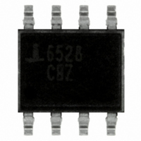
ISL6528CBZ-T Intersil, ISL6528CBZ-T Datasheet - Page 8

ISL6528CBZ-T
Manufacturer Part Number
ISL6528CBZ-T
Description
IC CTRLR PWM BUCK DUAL 8-SOIC
Manufacturer
Intersil
Datasheet
1.ISL6528CBZ-T.pdf
(13 pages)
Specifications of ISL6528CBZ-T
Pwm Type
Voltage Mode
Number Of Outputs
2
Frequency - Max
650kHz
Duty Cycle
100%
Voltage - Supply
4.5 V ~ 5.5 V
Buck
Yes
Boost
No
Flyback
No
Inverting
No
Doubler
No
Divider
No
Cuk
No
Isolated
No
Operating Temperature
0°C ~ 70°C
Package / Case
8-SOIC (3.9mm Width)
Frequency-max
650kHz
Peak Reflow Compatible (260 C)
Yes
Rohs Compliant
Yes
Lead Free Status / RoHS Status
Lead free / RoHS Compliant
Other names
ISL6528CBZ-TTR
Compensation Break Frequency Equations
Follow this procedure for selecting compensation
components by locating the poles and zeros of the
compensation network:
Figure 6 shows an asymptotic plot of the DC/DC converter’s
gain vs. frequency. The actual modulator gain has a high
gain peak dependent on the quality factor (Q) of the output
filter, which is not shown in Figure 6. Using the above
procedure should yield a compensation gain similar to the
curve plotted. The open loop error amplifier gain bounds the
compensation gain. Check the compensation gain at F
with the capabilities of the error amplifier.
Poles:
Zeros:
1. Set the loop gain (R2/R1) to provide a converter
2. Place the first compensation zero, F
3. Position the second compensation zero, F
4. Locate the first compensation pole, F
5. Position the second compensation pole at half the
6. Check gain against error amplifier’s open-loop gain.
7. Estimate phase margin; repeat if necessary.
FIGURE 6. ASYMPTOTIC BODE PLOT OF CONVERTER GAIN
8 .
100
-20
-40
-60
80
60
40
20
bandwidth of one quarter of the switching frequency.
filter double pole (~75% F
output filter double pole, F
ESR zero, F
converter switching frequency, F
0
F
F
F
F
P1
P2
Z2
Z1
10
MODULATOR
20
=
=
=
=
log
GAIN
------------------------------------------------------ -
2π
-----------------------------------
2π
------------------------------------------------------ -
2π
-----------------------------------
2π
100
R2
-------- -
R1
×
×
×
F
×
R
R
ESR
Z1
(
R
1
R1
2
3
1
2
×
×
×
+
.
1
1
F
C3
1K
--------------------- -
C1
C1
C1
R3
LC
F
FREQUENCY (Hz)
×
+
)
Z2
×
F
C2
C2
C3
ESR
10K
LC
8
LC
F
P1
).
.
100K
F
SW
P2
.
Z1
P1
, below the output
, at the output filter
1M
ERROR AMP GAIN
COMPENSATION
Z2
OPEN LOOP
20
LOOP GAIN
, at the
log
10M
GAIN
(EQ. 10)
(EQ. 11)
----------------- -
V
(EQ. 8)
(EQ. 9)
V IN
OSC
P2
ISL6528
The compensation gain uses external impedance networks
Z
loop. A stable control loop has a gain crossing with
-20dB/decade slope and a phase margin greater than 45°.
Include worst case component variations when determining
phase margin.
Application Guidelines
Layout Considerations
Layout is very important in high frequency switching
converter design. With power devices switching efficiently at
600kHz, the resulting current transitions from one device to
another cause voltage spikes across the interconnecting
impedances and parasitic circuit elements. These voltage
spikes can degrade efficiency, radiate noise into the circuit,
and lead to device overvoltage stress. Careful component
layout and printed circuit board design minimizes the voltage
spikes in the converters.
As an example, consider the turn-off transition of the PWM
MOSFET. Prior to turn-off, the MOSFET is carrying the full
load current. During turn-off, current stops flowing in the
MOSFET and is picked up by the lower Schottky diode. Any
parasitic inductance in the switched current path generates a
large voltage spike during the switching interval. Careful
component selection, tight layout of the critical components,
and short, wide traces minimizes the magnitude of voltage
spikes.
There are two sets of critical components in a DC/DC
converter using the ISL6528. The switching components are
the most critical because they switch large amounts of
energy, and therefore tend to generate large amounts of
noise. Next are the small signal components which connect
to sensitive nodes or supply critical bypass current and
signal coupling.
A multi-layer printed circuit board is recommended. Figure 7
shows the connections of the critical components in the
converter. Note that capacitors C
represent numerous physical capacitors. Dedicate one solid
layer, usually a middle layer of the PC board, for a ground
plane and make all critical component ground connections
through vias to this layer. Dedicate another solid layer as a
power plane and break this plane into smaller islands of
common voltage levels. Keep the metal runs from the
PHASE terminal to the output inductor short. The power
plane should support the input and output power nodes. Use
copper filled polygons on the top and bottom circuit layers for
the phase node. Use the remaining printed circuit layers for
small signal wiring. The wiring traces from the UGATE pin to
the MOSFET gate should be kept short and wide enough to
easily handle the 1A of drive current.
The switching components should be placed close to the
ISL6528 first. Minimize the length of the connections
between the input capacitors, C
FB
and Z
IN
to provide a stable, high bandwidth (BW) overall
IN
IN
, and the power switches
and C
OUT
could each
March 9, 2006
FN9038.4


