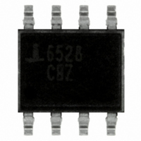
ISL6528CBZ-T Intersil, ISL6528CBZ-T Datasheet - Page 11

ISL6528CBZ-T
Manufacturer Part Number
ISL6528CBZ-T
Description
IC CTRLR PWM BUCK DUAL 8-SOIC
Manufacturer
Intersil
Datasheet
1.ISL6528CBZ-T.pdf
(13 pages)
Specifications of ISL6528CBZ-T
Pwm Type
Voltage Mode
Number Of Outputs
2
Frequency - Max
650kHz
Duty Cycle
100%
Voltage - Supply
4.5 V ~ 5.5 V
Buck
Yes
Boost
No
Flyback
No
Inverting
No
Doubler
No
Divider
No
Cuk
No
Isolated
No
Operating Temperature
0°C ~ 70°C
Package / Case
8-SOIC (3.9mm Width)
Frequency-max
650kHz
Peak Reflow Compatible (260 C)
Yes
Rohs Compliant
Yes
Lead Free Status / RoHS Status
Lead free / RoHS Compliant
Other names
ISL6528CBZ-TTR
load current when the base is fed with the minimum driver
output current.
The main criteria for selection of the linear regulator pass
transistor is package selection for efficient removal of heat.
Select a package and heatsink that maintains the junction
temperature below the rating with a maximum expected
ambient temperature.
The power dissipated in a linear regulator is:
where I
nominal output voltage of the linear regulator.
Diode Selection (D1)
Rectifier D1 conducts when MOSFET Q1 is off. The diode
should be a Schottky type for low power losses. The power
dissipation in the Schottky rectifier is approximated by:
where I
converter, V
the duty cycle of the converter (defined as V
In addition to power dissipation, package selection and
heatsink requirements are the main design trade-offs in
choosing a Schottky rectifier. Since the three factors are
interrelated, the selection process is an iterative procedure.
The maximum junction temperature of the rectifier must
remain below the manufacturer’s specified value, typically
125°C. By using the package thermal resistance
specification and the Schottky power dissipation equation,
the junction temperature of the rectifier can be estimated. Be
sure to use the available airflow and ambient temperature to
determine the junction temperature rise.
Bootstrap Component Selection
External bootstrap components, a diode and capacitor, are
required to provide sufficient gate enhancement to the
MOSFET. The internal MOSFET gate driver is supplied by
the external bootstrap circuitry as shown in Figure 8. The
boot capacitor, C
referenced to the PHASE pin. This supply is refreshed each
cycle, when D1 conducts, to a voltage of VCC less the boot
diode drop, V
Just after the PWM switching cycle begins and the charge
transfer from the bootstrap capacitor to the gate capacitance
is complete, the voltage on the bootstrap capacitor is at its
lowest point during the switching cycle. The charge lost on
the bootstrap capacitor will be equal to the charge
transferred to the equivalent gate-source capacitance of the
MOSFET as shown in Equation 19.
P
P
Q
LINEAR
CONDUCTION
GATE
O
O
=
≅
is the maximum output current and V
is the maximum output current of the PWM
C
I
O
BOOT
f
is the Schottky forward voltage drop, and D is
×
D2
(
≅
V
, plus the voltage rise across D1.
I
BOOT
IN
O
×
(
×
–
V
V
V
BOOT1
OUT
f
, develops a floating supply voltage
×
(
1 D
)
–
–
11
V
)
BOOT2
)
O
/V
OUT
IN
).
(EQ. 17)
is the
(EQ. 18)
(EQ. 19)
ISL6528
where Q
MOSFET, C
the bootstrap voltage immediately before turn-on, and
V
The bootstrap capacitor begins its refresh cycle when the
gate drive begins to turn off the MOSFET. A refresh cycle
ends when the MOSFET is turned on again, which varies
depending on the switching frequency and duty cycle.
The minimum bootstrap capacitance can be calculated by
rearranging Equation 19 and solving for C
Typical gate charge values for MOSFETs considered in
these types of applications range from 20–100nC. Since the
voltage drop across D2 is offset by the voltage drop across
D1, V
voltage drop across the bootstrap capacitor no greater than
1V during the on-time of the MOSFET. Initial calculations
with V
bootstrap capacitor range.
For example, consider a MOSFET is chosen with a
maximum gate charge, Q
drop across the bootstrap capacitor to 1V results in a value
of no less than 0.1µF. The tolerance of the ceramic capacitor
should also be considered when selecting the final bootstrap
capacitance value.
A fast recovery diode is recommended when selecting a
bootstrap diode to reduce the impact of reverse recovery
charge loss. Otherwise, the recovery charge, Q
have to be added to the gate charge of the MOSFET and
taken into consideration when calculating the minimum
bootstrap capacitance. Employing a Schottky diode over a
standard diode will also increase the gate drive voltage
available to enhance the MOSFET.
C
BOOT2
BOOT
BOOT1
BOOT2
≥
GATE
is the bootstrap voltage immediately after turn-on.
---------------------------------------------------- -
V
BOOT1
BOOT
is simply VCC (+5V). A good rule is to keep the
no less than 4V will quickly help narrow the
+5V
is the maximum total gate charge of the
Q
FIGURE 8. UPPER GATE DRIVE
ISL6528
VCC
GATE
D2
–
is the bootstrap capacitance, V
V
BOOT2
BOOT
g
, of 100nC. Limiting the voltage
UGATE
PHASE
C
BOOT
+3.3V
BOOT
Q1
D1
RR
.
BOOT1
, would
March 9, 2006
(EQ. 20)
FN9038.4
is


