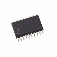
HIP6004ECBZ Intersil, HIP6004ECBZ Datasheet - Page 4

HIP6004ECBZ
Manufacturer Part Number
HIP6004ECBZ
Description
IC PWM CTRLR/VOLT OUT MON 20SOIC
Manufacturer
Intersil
Datasheet
1.HIP6004ECBZ.pdf
(13 pages)
Specifications of HIP6004ECBZ
Pwm Type
Voltage Mode
Number Of Outputs
1
Frequency - Max
1MHz
Duty Cycle
100%
Voltage - Supply
5 V ~ 12 V
Buck
Yes
Boost
No
Flyback
No
Inverting
No
Doubler
No
Divider
No
Cuk
No
Isolated
No
Operating Temperature
0°C ~ 70°C
Package / Case
20-SOIC (7.5mm Width)
Frequency-max
1MHz
Input Voltage
12V
Output Voltage
1.825V
Supply Voltage Range
10.8V To 13.2V
Digital Ic Case Style
SOIC
No. Of Pins
20
Operating Temperature Range
0°C To +70°C
Filter Terminals
SMD
Rohs Compliant
Yes
Control Mode
Voltage
Lead Free Status / RoHS Status
Lead free / RoHS Compliant
Available stocks
Company
Part Number
Manufacturer
Quantity
Price
Part Number:
HIP6004ECBZ
Manufacturer:
INTERSIL
Quantity:
20 000
Company:
Part Number:
HIP6004ECBZ-T
Manufacturer:
Intersil
Quantity:
1 000
Company:
Part Number:
HIP6004ECBZ-T
Manufacturer:
HARRIS
Quantity:
703
Part Number:
HIP6004ECBZ-T
Manufacturer:
INTERSIL
Quantity:
20 000
Typical Performance Curves
Functional Pin Descriptions
VSEN (Pin 1)
This pin is connected to the converter’s output voltage. The
PGOOD and OVP comparator circuits use this signal to
report output voltage status and for overvoltage protection.
OCSET (Pin 2)
Connect a resistor (R
upper MOSFET. R
(I
set the converter overcurrent (OC) trip point according to the
following equation:
An over-current trip cycles the soft-start function.
SS (Pin 3)
Connect a capacitor from this pin to ground. This capacitor,
along with an internal 10µA current source, sets the soft-
start interval of the converter.
VID25mV-VID3 (Pins 4-8)
VID25mV - VID3 are the input pins to the 5-bit DAC. The
states of these five pins program the internal voltage
I
PEAK
OCSET
1000
100
10
10
=
), and the upper MOSFET on-resistance (r
FIGURE 1. R
I
---------------------------------------------------- -
OCSET
VID25mV
R
OCSET
r
T
COMP
TO +12V
DS ON
VSEN
PULLUP
VID0
VID1
VID2
VID3
x R
SS
FB
(
OCSET
SWITCHING FREQUENCY (kHz)
OCSET
T
10
OCSET
)
1
2
3
4
5
6
7
8
9
RESISTANCE vs FREQUENCY
, an internal 200µA current source
) from this pin to the drain of the
4
100
R
T
PULLDOWN TO V
20
19
18
17
16
15
14
13
12
11
RT
OVP
VCC
LGATE
PGND
BOOT
UGATE
PHASE
PGOOD
GND
SS
DS(ON)
1000
)
HIP6004E
reference (DACOUT). The level of DACOUT sets the
converter output voltage. It also sets the PGOOD and OVP
thresholds. Table 1 specifies DACOUT for the all
combinations of DAC inputs.
COMP (Pin 9) and FB (Pin 10)
COMP and FB are the available external pins of the error
amplifier. The FB pin is the inverting input of the error
amplifier and the COMP pin is the error amplifier output.
These pins are used to compensate the voltage-control
feedback loop of the converter.
GND (Pin 11)
Signal ground for the IC. All voltage levels are measured with
respect to this pin.
PGOOD (Pin 12)
PGOOD is an open collector output used to indicate the
status of the converter output voltage. This pin is pulled low
when the converter output is not within ±10% of the
DACOUT reference voltage.
PHASE (Pin 13)
Connect the PHASE pin to the upper MOSFET source. This
pin is used to monitor the voltage drop across the MOSFET
for overcurrent protection. This pin also provides the return
path for the upper gate drive.
UGATE (Pin 14)
Connect UGATE to the upper MOSFET gate. This pin
provides the gate drive for the upper MOSFET.
BOOT (Pin 15)
This pin provides bias voltage to the upper MOSFET driver.
A bootstrap circuit may be used to create a BOOT voltage
suitable to drive a standard N-Channel MOSFET.
80
70
60
50
40
30
20
10
FIGURE 2. BIAS SUPPLY CURRENT vs FREQUENCY
0
100
C
UPPER
200
= C
300
SWITCHING FREQUENCY (kHz)
LOWER
400
= C
500
GATE
600
C
GATE
C
C
GATE
700
GATE
= 3300pF
= 10pF
= 1000pF
800
900
1000


