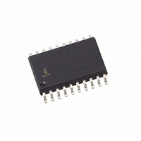
HIP6004ECBZ Intersil, HIP6004ECBZ Datasheet - Page 8

HIP6004ECBZ
Manufacturer Part Number
HIP6004ECBZ
Description
IC PWM CTRLR/VOLT OUT MON 20SOIC
Manufacturer
Intersil
Datasheet
1.HIP6004ECBZ.pdf
(13 pages)
Specifications of HIP6004ECBZ
Pwm Type
Voltage Mode
Number Of Outputs
1
Frequency - Max
1MHz
Duty Cycle
100%
Voltage - Supply
5 V ~ 12 V
Buck
Yes
Boost
No
Flyback
No
Inverting
No
Doubler
No
Divider
No
Cuk
No
Isolated
No
Operating Temperature
0°C ~ 70°C
Package / Case
20-SOIC (7.5mm Width)
Frequency-max
1MHz
Input Voltage
12V
Output Voltage
1.825V
Supply Voltage Range
10.8V To 13.2V
Digital Ic Case Style
SOIC
No. Of Pins
20
Operating Temperature Range
0°C To +70°C
Filter Terminals
SMD
Rohs Compliant
Yes
Control Mode
Voltage
Lead Free Status / RoHS Status
Lead free / RoHS Compliant
Available stocks
Company
Part Number
Manufacturer
Quantity
Price
Part Number:
HIP6004ECBZ
Manufacturer:
INTERSIL
Quantity:
20 000
Company:
Part Number:
HIP6004ECBZ-T
Manufacturer:
Intersil
Quantity:
1 000
Company:
Part Number:
HIP6004ECBZ-T
Manufacturer:
HARRIS
Quantity:
703
Part Number:
HIP6004ECBZ-T
Manufacturer:
INTERSIL
Quantity:
20 000
The PWM wave is smoothed by the output filter (L
The modulator transfer function is the small-signal transfer
function of V
Gain and the output filter (L
break frequency at F
the modulator is simply the input voltage (V
peak-to-peak oscillator voltage ∆V
Modulator Break Frequency Equations
The compensation network consists of the error amplifier
(internal to the HIP6004E) and the impedance networks Z
and Z
a closed loop transfer function with the highest 0dB crossing
frequency (f
is the difference between the closed loop phase at f
180 degrees. The equations below relate the compensation
network’s poles, zeros and gain to the components (R
R
locating the poles and zeros of the compensation network:
F LC
∆V
1. Pick Gain (R
3. Place 2
4. Place 1
5. Place 2
6. Check Gain against Error Amplifier’s Open-Loop Gain.
7. Estimate Phase Margin - Repeat if Necessary.
2. Place 1
3
FIGURE 7. VOLTAGE-MODE BUCK CONVERTER
, C
OSC
=
FB
1
------------------------------------------ -
2π x
, C
. The goal of the compensation network is to provide
OSC
2
ST
, and C
ND
ST
ND
0dB
OUT
COMPARATOR
L O x C O
1
COMPENSATION DESIGN
Zero Below Filter’s Double Pole (~75% F
ERROR
AMP
DETAILED COMPENSATION COMPONENTS
Pole at the ESR Zero.
V
HIP6004E
Zero at Filter’s Double Pole.
Pole at Half the Switching Frequency.
) and adequate phase margin. Phase margin
E/A
2
PWM
/V
/R
3
E/A
Z
+
-
) in Figure 7. Use these guidelines for
1
FB
-
+
COMP
LC
) for desired converter bandwidth.
C
. This function is dominated by a DC
1
REFERENCE
and a zero at F
C
DACOUT
-
+
2
O
DRIVER
DRIVER
R
F ESR
and C
Z
2
8
IN
OSC
FB
=
O
Z
------------------------------------------- -
2π x ESR x C O
FB
), with a double pole
.
ESR
PHASE
(PARASITIC)
V
C
IN
3
IN
L
Z
R
. The DC Gain of
1
IN
O
1
) divided by the
R
ESR
C
3
O
V
O
OUT
and C
0dB
LC
V
1
OUT
, R
and
).
O
IN
2
HIP6004E
).
,
Compensation Break Frequency Equations
Figure 8 shows an asymptotic plot of the DC-DC converter’s
gain vs. frequency. The actual Modulator Gain has a high gain
peak due to the high Q factor of the output filter and is not
shown in Figure 8. Using the above guidelines should give a
Compensation Gain similar to the curve plotted. The open
loop error amplifier gain bounds the compensation gain.
Check the compensation gain at F
the error amplifier. The Closed Loop Gain is constructed on
the log-log graph of Figure 8 by adding the Modulator Gain (in
dB) to the Compensation Gain (in dB). This is equivalent to
multiplying the modulator transfer function to the
compensation transfer function and plotting the gain.
The compensation gain uses external impedance networks
Z
loop. A stable control loop has a gain crossing with
-20dB/decade slope and a phase margin greater than 45
degrees. Include worst case component variations when
determining phase margin.
Component Selection Guidelines
Output Capacitor Selection
An output capacitor is required to filter the output and supply
the load transient current. The filtering requirements are a
function of the switching frequency and the ripple current.
The load transient requirements are a function of the slew
rate (di/dt) and the magnitude of the transient load current.
These requirements are generally met with a mix of
capacitors and careful layout.
Modern microprocessors produce transient load rates above
1A/ns. High frequency capacitors initially supply the transient
and slow the current load rate seen by the bulk capacitors.
F
F
FIGURE 8. ASYMPTOTIC BODE PLOT OF CONVERTER GAIN
FB
Z1
Z2
100
-20
-40
-60
80
60
40
20
0
and Z
=
=
----------------------------------- -
2π x R
------------------------------------------------------ -
2π x R
10
(R
20LOG
2
MODULATOR
IN
/R
(
1
1
to provide a stable, high bandwidth (BW) overall
)
GAIN
2
100
1
x C
1
+
R
1
3
) x C
1K
F
Z1
F
FREQUENCY (Hz)
3
LC
F
Z2
10K
F
F
F
P1
P2
F
P1
ESR
(V
P2
=
=
100K
IN
20LOG
F
-------------------------------------------------------- -
2π x R
----------------------------------- -
2π x R
/∆V
with the capabilities of
P2
OSC
OPEN LOOP
ERROR AMP GAIN
1
1M
)
2
3
x
x C
1
COMPENSATION
CLOSED LOOP
C
--------------------- -
C
3
1
1
10M
GAIN
+
x C
GAIN
C
2
2


