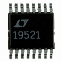
LT1952EGN-1#PBF Linear Technology, LT1952EGN-1#PBF Datasheet - Page 10

LT1952EGN-1#PBF
Manufacturer Part Number
LT1952EGN-1#PBF
Description
IC CTLR PWM SGL SWITCH 16-SSOP
Manufacturer
Linear Technology
Datasheet
1.LT1952EGNPBF.pdf
(24 pages)
Specifications of LT1952EGN-1#PBF
Pwm Type
Current Mode
Number Of Outputs
1
Frequency - Max
560kHz
Duty Cycle
90%
Voltage - Supply
6.82 V ~ 25 V
Buck
No
Boost
No
Flyback
Yes
Inverting
No
Doubler
No
Divider
No
Cuk
No
Isolated
Yes
Operating Temperature
-40°C ~ 125°C
Package / Case
16-SSOP
Frequency-max
560kHz
Lead Free Status / RoHS Status
Lead free / RoHS Compliant
Available stocks
Company
Part Number
Manufacturer
Quantity
Price
OPERATION
LT1952/LT1952-1
Introduction
The LT1952/LT1952-1 are current mode synchronous
PWM controllers optimized for control of the simplest
forward converter topology—using only one primary
MOSFET. The LT1952/LT1952-1 are ideal for 25W to 500W
power systems where very high effi ciency and reliability,
low complexity and cost are required in a small space.
Key features of the LT1952/LT1952-1 include an adaptive
maximum duty cycle clamp for the single primary MOSFET.
An additional output signal is included for synchronous
rectifi er control. A precision 107mV threshold senses
overcurrent conditions and triggers Soft-Start for low
stress short-circuit protection and control. The key
functions of the LT1952/LT1952-1 are shown in the Block
Diagram in Figure 2.
Part Start-up
In normal operation the SD_V
and the V
allow the part to turn on. This combination of pin voltages
allows the 2.5V V
LT1952/LT1952-1 control circuitry and providing up to
2.5mA external drive. SD_V
externally programming an undervoltage lockout (UVLO)
threshold on the system input voltage. Hysteresis on
the UVLO threshold can also be programmed since the
SD_V
after part turn on.
With the LT1952/LT1952-1 turned on, the V
as low as 8.75V (6.5V LT1952-1) before part shutdown
occurs. This V
LT1952-1) combined with low 460μA (400μA LT1952-1)
start-up input current allows low power start-up using
a resistor/capacitor network from system V
the V
to prevent V
an auxiliary winding in the converter takes over supply
to the V
Output Drivers
The LT1952/LT1952-1 have two outputs, SOUT and OUT.
The OUT pin provides a ±1A peak MOSFET gate drive
clamped to 13V. The SOUT pin has a ±50mA peak drive
10
IN
SEC
pin (Figure 3). The V
IN
IN
pin draws 11μA just before part turn on and 0μA
pin.
pin must exceed 14.25V (7.75V LT1952-1) to
IN
falling below its turn off threshold before
IN
REF
pin hysteresis (5.5V LT1952; 1.25V
pin to become active, supplying the
SEC
IN
SEC
capacitor value is chosen
threshold can be used for
pin must exceed 1.32V
IN
pin can drop
IN
to supply
clamped to 12V and provides sync signal timing for
synchronous rectifi cation control.
For SOUT and OUT turn on, a PWM latch is set at the start
of each main oscillator cycle. OUT turn on is delayed from
SOUT turn on by a time t
grammed using a resistor from the DELAY pin to ground
and is used to set the timing control of the secondary
synchronous rectifi ers for optimum effi ciency.
SOUT and OUT turn off at the same time each cycle by
one of three methods:
(1) MOSFET peak current sense at I
(2) Adaptive maximum duty cycle clamp reached during
load/line transients
(3) Maximum duty cycle reset of the PWM latch
During any of the following conditions—low V
SD_V
start event is latched and both SOUT and OUT turn off
immediately (Figure 1).
Leading Edge Blanking
To prevent MOSFET switching noise causing premature turn
off of SOUT or OUT, programmable leading edge blanking
exists. This means both the current sense comparator
and overcurrent comparator outputs are ignored during
MOSFET turn on and for an extended period after the OUT
leading edge (Figure 6). The extended blanking period is
programmable by adjusting a resistor from the BLANK
pin to ground.
Adaptive Maximum Duty Cycle Clamp
(Volt-Second Clamp)
For forward converter applications using the simplest
topology of a single MOSFET on the primary, a maximum
switch duty cycle clamp which adapts to transformer input
voltage is necessary for reliable control of the MOSFET. This
volt-second clamp provides a safeguard for transformer
reset that prevents transformer saturation. Instantaneous
load changes can cause the converter loop to demand
maximum duty cycle. If the maximum duty cycle of the
switch is too great, the transformer reset voltage can
exceed the voltage rating of the primary-side MOSFET with
SEC
or overcurrent detection at the OC pin—a soft-
DELAY
(Figure 2). t
SENSE
pin
DELAY
IN
is pro-
, low
19521fd


