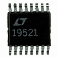
LT1952EGN-1#PBF Linear Technology, LT1952EGN-1#PBF Datasheet - Page 8

LT1952EGN-1#PBF
Manufacturer Part Number
LT1952EGN-1#PBF
Description
IC CTLR PWM SGL SWITCH 16-SSOP
Manufacturer
Linear Technology
Datasheet
1.LT1952EGNPBF.pdf
(24 pages)
Specifications of LT1952EGN-1#PBF
Pwm Type
Current Mode
Number Of Outputs
1
Frequency - Max
560kHz
Duty Cycle
90%
Voltage - Supply
6.82 V ~ 25 V
Buck
No
Boost
No
Flyback
Yes
Inverting
No
Doubler
No
Divider
No
Cuk
No
Isolated
Yes
Operating Temperature
-40°C ~ 125°C
Package / Case
16-SSOP
Frequency-max
560kHz
Lead Free Status / RoHS Status
Lead free / RoHS Compliant
Available stocks
Company
Part Number
Manufacturer
Quantity
Price
PIN FUNCTIONS
LT1952/LT1952-1
COMP (Pin 1): Output Pin of the Error Amplifi er. The error
amplifi er is an op amp, allowing various compensation
networks to be connected between the COMP pin and
FB pin for optimum transient response. The voltage on
this pin corresponds to the peak current of the external
FET. Full operating voltage range is between 0.8V and
2.5V corresponding to 0mV to 220mV at the I
For applications using the 100mV OC pin for overcurrent
detection, typical operating range for the COMP pin is
0.8V to 1.6V. For isolated applications where COMP is
controlled by an opto-coupler, the COMP pin output drive
can be disabled with FB = V
current to (COMP – 0.7)/40k.
FB (Pin 2): Monitors the output voltage via an external
resistor divider and is compared with an internal 1.23V
reference by the error amplifi er. FB connected to V
disables error amplifi er output.
R
frequency of the IC between 100kHz and 500kHz. Nominal
voltage on the R
SYNC (Pin 4): Used to Synchronize the Internal Oscillator
to an External Signal. It is directly logic compatible and
can be driven with any signal between 10% and 90% duty
cycle. If unused, the pin can be left open or connected to
ground.
SS_MAXDC (Pin 5): External resistor divider from V
sets maximum duty cycle clamp (SS_MAXDC = 1.84V,
SD_V
SS_MAXDC pin in combination with external resistor
divider sets soft-start timing.
V
supplies control circuitry in the IC. Capable of sourcing up
to 2.5mA drive for external use. Bypass to ground with a
0.1μF ceramic capacitor.
SD_V
its accurate 1.32V threshold, is used to turn off the IC
and reduce current drain from V
connected to system input voltage through a resistor
divider to defi ne undervoltage lockout (UVLO) and to
provide a Volt-Second clamp on the OUT pin. A 10μA pin
current hysteresis allows external programming of UVLO
hysteresis.
8
REF
OSC
(Pin 6): The output of an internal 2.5V reference which
(Pin 3): A resistor to ground programs the operating
SEC
SEC
(Pin 7): The SD_V
= 1.32V gives 72% duty cycle). Capacitor on
OSC
pin is 1.0V.
REF
SEC
, reducing the COMP pin
pin, when pulled below
IN
. The SD_V
SENSE
SEC
pin is
pin.
REF
REF
GND (Pin 8): Analog Ground.
BLANK (Pin 9): A resistor to ground adjusts the extended
blanking period of the overcurrent and current sense
amplifi er outputs during FET turn on—to prevent false
current limit trip. Increasing the resistor value increases
the blanking period.
I
Loop. Connect this pin to the sense resistor in the source
of the external power MOSFET. A resistor in series with
the I
OC (Pin 11): An accurate 107mV threshold, independent
of duty cycle, for overcurrent detection and trigger of
soft-start. Connect this pin directly to the sense resistor
in the source of the external power MOSFET.
DELAY (Pin 12): A resistor to ground adjusts the delay
period between SOUT rising edge and OUT rising edge.
Used to maximize effi ciency in forward converter applica-
tions by adjusting the control timing of secondary side
synchronous rectifi er MOSFETs. Increasing the resistor
value increases the delay period.
PGND (Pin 13): Power Ground.
OUT (Pin 14): Drives the Gate of an N-channel MOSFET
between 0V and V
OUT pin set by an internal clamp. Active pull-off exists in
shutdown (see electrical specifi cation).
V
decoupled to ground. An internal undervoltage lockout
threshold exists for V
and 8.75V off for the LT1952. The LT1952-1 has lower
undervoltage lockout thresholds set at 7.75V on and
6.5V off.
SOUT (Pin 16): Switched Output in Phase with OUT Pin.
Provides sync signal for control of secondary side FETs
in forward converter applications requiring highly effi cient
synchronous rectifi cation. SOUT is actively clamped to
12V. Active pull-off exists in shutdown (see electrical
specifi cation).
SENSE
IN
(Pin 15): Input Supply for the Part. It must be closely
SENSE
(Pin 10): The Current Sense Input for the Control
pin programs slope compensation.
IN
with a maximum limit of 13V on
IN
at approximately 14.25V on
19521fd


