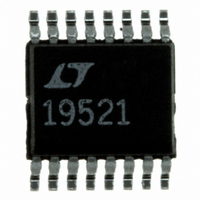
LT1952EGN-1#PBF Linear Technology, LT1952EGN-1#PBF Datasheet - Page 23

LT1952EGN-1#PBF
Manufacturer Part Number
LT1952EGN-1#PBF
Description
IC CTLR PWM SGL SWITCH 16-SSOP
Manufacturer
Linear Technology
Datasheet
1.LT1952EGNPBF.pdf
(24 pages)
Specifications of LT1952EGN-1#PBF
Pwm Type
Current Mode
Number Of Outputs
1
Frequency - Max
560kHz
Duty Cycle
90%
Voltage - Supply
6.82 V ~ 25 V
Buck
No
Boost
No
Flyback
Yes
Inverting
No
Doubler
No
Divider
No
Cuk
No
Isolated
Yes
Operating Temperature
-40°C ~ 125°C
Package / Case
16-SSOP
Frequency-max
560kHz
Lead Free Status / RoHS Status
Lead free / RoHS Compliant
Available stocks
Company
Part Number
Manufacturer
Quantity
Price
APPLICATIONS INFORMATION
Bus Converter: Optimum Output Voltage Tolerance
The Bus Converter applications shown on page 1 and in
Figure 16, provide semi-regulated isolated outputs without
the need for an optocoupler, optocoupler driver, reference or
feedback network. The LT1952/LT1952-1Volt-Second clamp
adjusts switch duty cycle inversely proportional to input
voltage to provide an output voltage that is regulated against
input line variations. Some bus converters use a switch duty
cycle limit which causes output voltage variation of typically
±33% over a 2:1 input voltage range. The LT1952/LT1952-1
typically provide a ±10% output variation for the same input
variation. Typical output tolerance is further improved for the
LT1952 by inserting a resistor from the system input voltage
to the SS_MAXDC pin (Rx in Figure 19).
The LT1952/LT1952-1 electrical specifi cations for the OUT
Max Duty Cycle Clamp show typical switch duty cycle to
move from 72% to 33% for a 2x change of input voltage
(SS_MAXDC pin = 1.84V). Since output voltage regulation
follows V
72% to 36% (for a 2x input voltage change) provides
minimal output voltage variation for the LT1952/LT1952-1
bus converter. To achieve this, an SS_MAXDC pin voltage
increase of 1.09x (36/33) would be required at high input
line. A resistor Rx inserted between the SS_MAXDC pin
and system input voltage (Figure 19) increases SS_MAXDC
voltage as input voltage increases, minimizing output
voltage variation over a 2:1 input voltage change.
The following steps determine values for Rx, R
(1)Program switch duty cycle at minimum system input
(a)R
voltage (V
start pull-down)
Figure 19. Optimal Programming of Maximum Duty
Cycle Clamp for Bus Converter Applications (Adding Rx)
T(1)
= 10k (minimum allowed to still guarantee soft-
IN
• Duty Cycle, a switch duty cycle change of
CLAMP ADJUST INPUT
VOLT-SECOND
S(MIN)
CLAMP INPUT
VOLT-SECOND
)
INPUT VOLTAGE
SYSTEM
R1
R2
Information furnished by Linear Technology Corporation is believed to be accurate and reliable.
However, no responsibility is assumed for its use. Linear Technology Corporation makes no representa-
tion that the interconnection of its circuits as described herein will not infringe on existing patent rights.
Rx
R
B
R
T
SD_V
SS_MAXDC
V
REF
LT1952-1
LT1952/
SEC
1952 F19
T
and R
B
:
(b)Select switch duty cycle for the Bus Converter for a
(c)Calculate R
(2)Calculate Rx:
(3)The addition of Rx causes an increase in the original
(a)SS2 = SS1 – [(V
(b)R
(4)The thevinin resistance R
Example:
For a Bus Converter running from 36V to 72V input,
V
choose R
duty cycle at V
S(MIN)
given output voltage at V
voltage (SS1) (See Applications Information “Program-
ming Maximum Duty Cycle Clamp”)
Rx = ([V
R
cycle (V
programmed SS_MAXDC voltage SS1. A new value for
R
voltage (SS2) to correct for this offset:
should be re-established for R
(a) R
(b) R
where R
R
R
SS_MAXDC correction = 36%/33% = 1.09
Rx = [(72V – 36V)/(1.84 • 0.09)] • 7.4k = 1.6M
SS2 = 1.84 – [(36V – 1.84) • 7.4k/1.6M] = 1.682V
R
R
R
R
R
THEV(1)
THEV(1)
THEV(2)
THEV(1)
T
B(1)
B(1)
B(2)
B
B(2)
(fi nal value) = 10k • 1.104 = 11k
(fi nal value) = 20.6k • 1.104 = 22.7k (choose 22.6k)
B
T
should be calculated to provide a lower SS_MAXDC
= 36V, V
= [1.84V/(2.5V – 1.84V)] • 10k = 28k
= [1.682/(2.5 – 1.682)] • 10k = 20.6k
= [SS2/(2.5 – SS2)] • R
T(1)
(fi nal value) = R
(fi nal value) = R
S(MAX)
THEV(2)
/R
S(MAX)
= [28k • 10k/(28k + 10k)] = 7.4k
= [20.6k • 10k/(20.6k + 10k)] = 6.7k
= R
THEV(2)
= 10k, SS_MAXDC = SS1 = 1.84V (for 72%
B(1)
S(MIN
B(1)
S(MAX)
)/actual duty cycle (V
– V
= [SS1/(2.5 – SS1)] • R
= R
S(MIN)
• R
) = 36V)
= 7.4k/6.7k = 1.104
S(MIN)
B(2)
T(1)
LT1952/LT1952-1
= 72V.
T(1)
B(2)
S(MIN)
– SS1) • R
/(R
• R
]/[SS1 • (X – 1)]) • R
THEV(1)
T(1)
B(1)
• (R
• (R
and calculate SS_MAXDC
T(1)
/(R
T
THEV(1)
+ R
THEV(1)
and R
B(2)
used to calculate Rx
THEV(1)
T(1)
S(MAX)
+ R
/R
), X = ideal duty
/R
B
:
T(1)
THEV(2)
THEV(2)
T(1)
/Rx]
)
)
THEV(1)
23
)
)
19521fd


