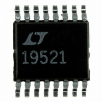
LT1952EGN-1#PBF Linear Technology, LT1952EGN-1#PBF Datasheet - Page 11

LT1952EGN-1#PBF
Manufacturer Part Number
LT1952EGN-1#PBF
Description
IC CTLR PWM SGL SWITCH 16-SSOP
Manufacturer
Linear Technology
Datasheet
1.LT1952EGNPBF.pdf
(24 pages)
Specifications of LT1952EGN-1#PBF
Pwm Type
Current Mode
Number Of Outputs
1
Frequency - Max
560kHz
Duty Cycle
90%
Voltage - Supply
6.82 V ~ 25 V
Buck
No
Boost
No
Flyback
Yes
Inverting
No
Doubler
No
Divider
No
Cuk
No
Isolated
Yes
Operating Temperature
-40°C ~ 125°C
Package / Case
16-SSOP
Frequency-max
560kHz
Lead Free Status / RoHS Status
Lead free / RoHS Compliant
Available stocks
Company
Part Number
Manufacturer
Quantity
Price
OPERATION
catastrophic damage. Many converters solve this problem
by limiting the operational duty cycle of the MOSFET to
50% or less—or by using a fi xed (non-adaptive) maximum
duty cycle clamp with very large voltage rated MOSFETs.
The LT1952/LT1952-1 provide a volt-second clamp to
allow MOSFET duty cycles well above 50%. This gives
greater power utilization for the MOSFET, rectifi ers and
transformer resulting in less space for a given power
output. In addition, the volt-second clamp allows a reduced
voltage rating on the MOSFET resulting in lower RDS
for greater effi ciency. The volt-second clamp defi nes a
maximum duty cycle ‘guard rail’ which falls when system
input voltage increases.
The LT1952/LT1952-1 SD_V
provide a capacitorless, programmable volt-second clamp
solution. Some controllers with volt-second clamps control
switch maximum duty cycle by using an external capacitor
to program maximum switch ON time. Such techniques
have a volt-second clamp inaccuracy directly related to
the error of the external capacitor/pin capacitance and the
error/drift of the internal oscillator. The LT1952/LT1952-
1 use simple resistor ratios to implement a volt-second
clamp without the need for an accurate external capacitor
and with an order of magnitude less dependency on
oscillator error.
An increase of voltage at the SD_V
maximum duty cycle clamp to decrease. If SD_V
resistively divided down from transformer input voltage,
a volt-second clamp is realised. To adjust the initial
maximum duty cycle clamp, the SS_MAXDC pin voltage
is programmed by a resistor divider from the 2.5V V
pin to ground. An increase of programmed voltage on
SS_MAXDC pin provides an increase of switch maximum
duty cycle clamp.
Soft-Start
The LT1952/LT1952-1 provide true PWM soft-start by
using the SS_MAXDC pin to control soft-start timing. The
proportional relationship between SS_MAXDC voltage and
switch maximum duty cycle clamp allows the SS_MAXDC
pin to slowly ramp output voltage by ramping the maximum
switch duty cycle clamp—until switch duty cycle clamp
seamlessly meets the natural duty cycle of the converter.
SEC
and SS_MAXDC pins
SEC
pin causes the
SEC
REF
ON
is
A soft-start event is triggered whenever V
SD_V
threshold at OC pin is exceeded. Whenever a soft-start
event is triggered, switching at SOUT and OUT is stopped
immediately.
The SS_MAXDC pin is discharged and only released for
charging when it has fallen below it’s reset threshold
of 0.45V and all faults have been removed. Increasing
voltage on the SS_MAXDC pin above 0.8V will increase
switch maximum duty cycle. A capacitor to ground on
the SS_MAXDC pin in combination with a resistor divider
from V
Current Mode Topology (I
The LT1952/LT1952-1 current mode topology eases fre-
quency compensation requirements because the output
inductor does not contribute to phase delay in the regulator
loop. This current mode technique means that the error
amplifi er (nonisolated applications) or the optocoupler
(isolated applications) commands current (rather than
voltage) to be delivered to the output. This makes frequency
compensation easier and provides faster loop response
to output load transients.
A resistor divider from the application’s output voltage
generates a voltage at the inverting FB input of the LT1952/
LT1952-1 error amplifi er (or to the input of an external
optocoupler) and is compared to an accurate reference
(1.23V for LT1952/LT1952-1). The error amplifi er output
(COMP) defi nes the input threshold (I
sense comparator. COMP voltages between 0.8V (active
threshold) and 2.5V defi ne a maximum I
from 0mV to 220mV. By connecting I
resistor in series with the source of an external power
MOSFET, the MOSFET peak current trip point (turn off)
can be controlled by COMP level and hence by the output
voltage. An increase in output load current causing the
output voltage to fall, will cause COMP to rise, increasing
I
output. For isolated applications, the error amplifi er COMP
output can be disabled to allow the optocoupler to take
control. Setting FB = V
output, reducing pin current to (COMP – 0.7)/40k.
SENSE
SEC
REF
threshold, increasing the current delivered to the
is too low (UVLO), or a 107mV overcurrent
, defi nes the soft-start timing.
REF
LT1952/LT1952-1
disables the error amplifi er COMP
SENSE
Pin)
SENSE
SENSE
SENSE
) of the current
IN
to a sense
is too low,
threshold
11
19521fd


