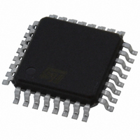
L5994 STMicroelectronics, L5994 Datasheet - Page 8

L5994
Manufacturer Part Number
L5994
Description
IC CTRLR PS ADJ TRPL-OUT 32-TQFP
Manufacturer
STMicroelectronics
Datasheet
1.L5994.pdf
(26 pages)
Specifications of L5994
Pwm Type
Current Mode
Number Of Outputs
3
Frequency - Max
345kHz
Duty Cycle
96%
Voltage - Supply
4.75 V ~ 25 V
Buck
Yes
Boost
No
Flyback
Yes
Inverting
No
Doubler
No
Divider
No
Cuk
No
Isolated
No
Operating Temperature
-40°C ~ 140°C
Package / Case
32-TQFP, 32-VQFP
Frequency-max
345kHz
Lead Free Status / RoHS Status
Lead free / RoHS Compliant
Available stocks
Company
Part Number
Manufacturer
Quantity
Price
L5994 - L5994A
the oscillator and the internal supply and differ for the pre-set output voltages.
Each converter can be turned on and off independently: RUN1 and RUN2 are control inputs which disable the
relevant section when a low logic level (below 0.8 V) is applied and enable its operation with a high logic level
(above 2.4 V). When both inputs are low the device is in stand-by condition and its current consumption is ex-
tremely reduced (less than 120mA over the entire input voltage range).
The device is able to regulate the desired output voltage in two different ways: classic PWM operation and Pulse
Skip operation (see the relevant sections).
Oscillator
The oscillator, which does not require any external timing component, controls the PWM switching frequency.
This can be either 200 or 300 kHz, depending on the logic state of the control pin OSC, or else can be synchro-
nized by an external oscillator.
If the OSC pin is grounded or connected to pin PREG5 (5V) the oscillator works at 200kHz. By connecting the
OSC pin to a 2.5 V voltage, 300 kHz operation will be selected. Moreover, if pin OSC is fed with an external
signal like the one shown in fig. 2, the oscillator will be synchronized by its falling edges.
Considering the spread of the oscillator, synchronization can be guaranteed for frequencies above 230kHz.
Even though a maximum frequency value is in practice imposed by efficiency considerations it should be noticed
that increasing frequency too much arises problems (noise, subharmonic oscillation, etc.) without significant
benefits in terms of external component size reduction and better dynamic performance.
The oscillator imposes a time interval (300 ns min.), during which the high-side MOSFET is definitely OFF, to
recharge the bootstrap capacitor (see "MOSFET's Drivers" section). This, implies a limit on the maximum duty
cycle (88.5%@fSW=300kHz, 92.6%@fsw=200kHz, worst case) which, in turn, imposes a limit on the minimum
operating input voltage.
Figure 2. Synchronization signal and operation
PWM Operation
The control loop does not employ a traditional error amplifier in favour of an error summing comparator which
sums the reference voltage, the feedback signal, the voltage drop across an external sense resistor and a slope
compensation ramp (to avoid subharmonic oscillation with duty cycles greater than 50%) with the appropriate
signs.
With reference to the schematic of fig. 3, the output latch of both controllers is set by every pulse coming from
8/26
H1GATE
H2GATE
OSC
5V
0V
300ns min.
t
t
t


