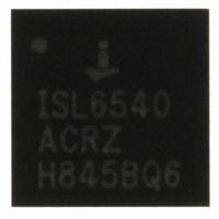
ISL6540IRZA-T Intersil, ISL6540IRZA-T Datasheet

ISL6540IRZA-T
Specifications of ISL6540IRZA-T
Related parts for ISL6540IRZA-T
ISL6540IRZA-T Summary of contents
Page 1
... ISL6540CRZ PVCC 16 ISL6540CRZA ISL6540CRZ LINDRV 15 ISL6540IRZA 14 *Add “-T” suffix for tape and reel. NOTE: These Intersil Pb-free plastic packaged products employ special Pb-free material sets, molding compounds/die attach materials, and 100% matte tin plate plus anneal (e3 termination finish, which is RoHS compliant and compatible with both SnPb and Pb-free soldering operations) ...
Page 2
Block Diagram 2 ISL6540 FN9214.1 July 23, 2008 ...
Page 3
Typical Application I (Internal Linear Regulator with Remote Sense) +3.3V to +20V C F1 VIN Internal 5.6V Bias Linear Regulator VFF VCC REFIN REFOUT PG C PG_DLY PG_DLY MARCTRL R OFS+ OFS+ R MARG ...
Page 4
Typical Application II (External Linear Regulator without Remote Sense) +3.3V to +20V DRV LINDRV VIN C F3 VFF REFOUT VCC REFIN PG_DLY PG_DLY MARCTRL R OFS+ OFS+ R MARG ...
Page 5
Typical Application III (Dual Data Rate I or II) VDDQ 1.8V or 2.5V 5V VIN R EN1 VFF EN2 F4 1K REFIN REFOUT 15nF DIMM PG_DLY PG_DLY MARCTRL R OFS+ OFS+ ...
Page 6
Absolute Maximum Ratings Input Voltage, VIN, VFF . . . . . . . . . . . . . . . . . . . . . . -0.3V to +22.0V Driver Bias Voltage, PVCC . . . . ...
Page 7
Electrical Specifications Recommended Operating Conditions, Unless Otherwise Noted (Continued) SYMBOL PARAMETER OSCILLATOR OSC Nominal Frequency Range RANGE ΔOSC Total Variation COM ΔOSC IND ΔV Ramp Amplitude OSC V Ramp Bottom OSC_MIN VFF Minimum Usable VFF Voltage PWM D Maximum Duty ...
Page 8
Electrical Specifications Recommended Operating Conditions, Unless Otherwise Noted (Continued) SYMBOL PARAMETER GATE DRIVERS R Ugate Source Resistance UGATE I Ugate Source Saturation Current UGATE R Ugate Sink Resistance UGATE I Ugate Sink Saturation Current UGATE R Lgate Source Resistance LGATE ...
Page 9
Functional Pin Description VSEN+ (Pin 1) This pin provides differential remote sense for the ISL6540 the positive input of a standard instrumentation amplifier topology with unity gain, and should connect to the positive rail of the load/processor. The ...
Page 10
LIN_DRV (Pin 15, External Linear Regulator Drive) This pin allows the use of an external pass element to power the IC for input voltages above 5.0V. It should be connected to GND when using an external 5V supply or the ...
Page 11
Functional Description Initialization The ISL6540 automatically initializes upon receipt of power without requiring any special sequencing of the input supplies. The Power-On Reset (POR) function continually monitors the input supply voltages (PVCC,VFF, VCC) and the voltage at the EN pin. ...
Page 12
UV and OV functionality is not enabled until the end of soft-start event is detected asynchronously and causes the high side MOSFET to turn off, the low ...
Page 13
... High Speed MOSFET Gate Driver The integrated driver has similar drive capability and features to Intersil's ISL6605 stand alone gate driver. The PWM tri-state feature helps prevent a negative transient on the output voltage when the output is being shut down. This ...
Page 14
OFS increased. In both modes the voltage difference between OFS+ and OFS- is then sensed with an instrumentation amplifier and is converted to the desired margining voltage by a 5:1 ratio. The maximum designed margining range ...
Page 15
VOUT (LOCAL) GND (LOCAL) VCC 800mV FIGURE 6. SIMPLIFIED UNITY GAIN DIFFERENITAL SENSING IMPLEMENTATION Application Guidelines Layout Considerations As in any high frequency switching converter, layout is very important. Switching current from one power device to another can generate voltage ...
Page 16
Figure 8 shows the circuit traces that require additional layout consideration. Use single point and ground plane construction for the circuits shown. Minimize any leakage current paths on the SS pin and locate the capacitor, C close to the SS ...
Page 17
OSC 1 0 -------------------------------------------- - R = ⋅ ⋅ MAX small capacitor, in Figure 10, can be added to filter C SEN out noise, typically is chosen so ...
Page 18
A stable control loop has a gain crossing with close to a -20dB/decade slope and a phase margin greater than 45°. Include worst case component variations when determining phase margin. The mathematical model presented makes a number of approximations and ...
Page 19
... Accordingly, the reader is cautioned to verify that data sheets are current before placing orders. Information furnished by Intersil is believed to be accurate and reliable. However, no responsibility is assumed by Intersil or its subsidiaries for its use; nor for any infringements of patents or other rights of third parties which may result from its use ...
Page 20
Package Outline Drawing L28.5x5 28 LEAD QUAD FLAT NO-LEAD PLASTIC PACKAGE Rev 2, 10/07 5.00 6 PIN 1 INDEX AREA (4X) 0.15 TOP VIEW ( 4. 65 TYP ) ( 3. 10) TYPICAL RECOMMENDED LAND PATTERN 20 ISL6540 A B ...


