L6756D STMicroelectronics, L6756D Datasheet - Page 20

L6756D
Manufacturer Part Number
L6756D
Description
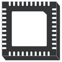
IC CTLR 2/3/4PH BUCK 40-VFQFPN
Manufacturer
STMicroelectronics
Datasheet
1.L6756DTR.pdf
(36 pages)
Specifications of L6756D
Applications
Controller, Intel VR10, VR11, VR11.1
Voltage - Input
12V
Number Of Outputs
4
Voltage - Output
0.3 ~ 1.6 V
Operating Temperature
0°C ~ 70°C
Mounting Type
Surface Mount
Package / Case
40-VFQFN, 40-VFQFPN
Output Voltage
3 V
Input Voltage
- 0.3 V to + 15 V
Switching Frequency
185 KHz to 215 KHz
Operating Temperature Range
- 40 C to + 150 C
Mounting Style
SMD/SMT
Lead Free Status / RoHS Status
Lead free / RoHS Compliant
Available stocks
Company
Part Number
Manufacturer
Quantity
Price
Output voltage positioning
5
5.1
20/36
Output voltage positioning
Output voltage positioning is performed by selecting the controller operation mode (VR10,
VR11 or VR11.1) and by programming the droop function and offset to the reference of both
the sections (See
voltage drop across the Inductors DCR. The current (I
directly proportional to the read current, causes the output voltage to vary according to the
external R
sunk through the VSEN pins causing the output voltage to be offset according to the
resistance R
L6756D allows to recover from GND losses in order to regulate remotely the programmed
voltage without any additional external components. In this way, the output voltage
programmed is regulated compensating for board and socket losses. Keeping the sense
traces parallel and guarded by a power plane results in common mode coupling for any
picked-up noise.
Both DROOP and OFFSET function can be disabled. In case DROOP effect is not desired,
the current information source from the DROOP pin may be used to implement a secondary
load indicator as reported in
Figure 6.
Phase # programming
L6756D implements a flexible 2 to 4 interleaved-phase converter. To program the desired
number of phase, refer to
For the disabled phase(s), the current reading pins need to be properly connected to avoid
errors in current-sharing and voltage-positioning: CSx needs to be connected to the regu-
lated output voltage while CSxN needs to be connected to CSx with the same R
used for the other phases.
FB
OS
Voltage positioning
resistor so implementing the desired load-line effect. A fixed current (I
connected.
Figure
6). The controller reads the current delivered by monitoring the
Table
Section
8.
5.3.
DROOP
) sourced from the DROOP pin,
G
resistor
OS
L6756D
) is


