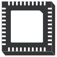
L6756D STMicroelectronics, L6756D Datasheet - Page 9

L6756D
Manufacturer Part Number
L6756D
Description
IC CTLR 2/3/4PH BUCK 40-VFQFPN
Manufacturer
STMicroelectronics
Datasheet
1.L6756DTR.pdf
(36 pages)
Specifications of L6756D
Applications
Controller, Intel VR10, VR11, VR11.1
Voltage - Input
12V
Number Of Outputs
4
Voltage - Output
0.3 ~ 1.6 V
Operating Temperature
0°C ~ 70°C
Mounting Type
Surface Mount
Package / Case
40-VFQFN, 40-VFQFPN
Output Voltage
3 V
Input Voltage
- 0.3 V to + 15 V
Switching Frequency
185 KHz to 215 KHz
Operating Temperature Range
- 40 C to + 150 C
Mounting Style
SMD/SMT
Lead Free Status / RoHS Status
Lead free / RoHS Compliant
Available stocks
Company
Part Number
Manufacturer
Quantity
Price
L6756D
Table 2.
Pin#
12
13
14
15
16
17
18
19
20
21
22
23
24
25
26
27
COMP
ROSC
VDRP
Name
VSEN
CS1N
CS2N
CS3N
CS4N
GND
FBG
VFB
ILIM
CS1
CS2
CS3
LTB
Pin description (continued)
Oscillator pin. It allows programming the switching frequency F
channel: the equivalent switching frequency at the load side results in being
multiplied by the phase number N.
Frequency is programmed according to the resistor connected from the pin to
GND or VCC with a gain of 10 kHz/µA. Leaving the pin floating programs a
switching frequency of 200 kHz per phase.
Over current SET pin. Connect to GND through a R
threshold. this pin sources a copy of the DROOP current; OC is set when the
voltage at the pin crosses 1.7 V (typ). See
All the internal references are referred to this pin. Connect to the PCB Signal
Ground.
Load transient boost Technology
Remote ground sense. Connect to the negative side of the load to perform
remote sense.
Output voltage monitor, manages OVP and UVP protections. Connect to the
positive side of the load to perform remote sense.
A fixed 50 μA current is sunk through this pin to implement small positive offset
for the regulated voltage. See
Error Amplifier Output.
Connect with an R
low this pin.
error amplifier inverting input.
Connect with a resistor R
A current proportional to the total current read is sourced from this pin
according to the current reading gain.
Short to VFB to implement voltage positioning or connect to GND through a
resistor and filter with 1 nF capacitor to implement an additional load indicator.
Channel 1 current sense negative input. Connect through a Rg resistor to the
output-side of the channel inductor.
Channel 1 current sense positive input. Connect through an R-C filter to the
phase-side of the channel 1 inductor.
Channel 2 current sense negative input. Connect through a Rg resistor to the
output-side of the channel inductor. When working at 2 phase, still connect
through Rg to CS2 and then to the regulated voltage.
Channel 2 current sense positive input. Connect through an R-C filter to the
phase-side of the channel 2 inductor. When working at 2 phase, short to the
regulated voltage.
Channel 3 current sense negative input. Connect through a Rg resistor to the
output-side of the channel inductor.
Channel 3 current sense positive input. Connect through an R-C filter to the
phase-side of the channel 3 inductor.
Channel 4 current sense negative input. Connect through a Rg resistor to the
output-side of the channel inductor. When working at 2 or 3 phase, still connect
through Rg to CS3 and then to the regulated voltage.
F
- C
F
// C
FB
H
to VSEN and with an R
Pins description and connection diagrams
to VFB. The device cannot be disabled by pulling
Section 5.4
®
Function
input pin. See
for details.
Section 6.4
Section 9.2
F
ILIM
- C
for details.
resistor to set the OC
F
// C
for details.
H
SW
to COMP.
of each
9/36


