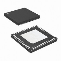
ISL6336ACRZ Intersil, ISL6336ACRZ Datasheet - Page 30

ISL6336ACRZ
Manufacturer Part Number
ISL6336ACRZ
Description
IC CTRLR PWM 6PHASE BUCK 48-QFN
Manufacturer
Intersil
Datasheet
1.ISL6336ACRZ.pdf
(31 pages)
Specifications of ISL6336ACRZ
Applications
Controller, Intel VR11.1
Voltage - Input
3 ~ 12 V
Number Of Outputs
1
Voltage - Output
0.5 ~ 1.6 V
Operating Temperature
0°C ~ 70°C
Mounting Type
Surface Mount
Package / Case
48-VQFN
Lead Free Status / RoHS Status
Lead free / RoHS Compliant
Available stocks
Company
Part Number
Manufacturer
Quantity
Price
Company:
Part Number:
ISL6336ACRZ
Manufacturer:
INTERSIL
Quantity:
280
Layout Considerations
The following layout strategies are intended to minimize the
impact of board parasitic impedances on converter
performance and to optimize the heat-dissipating capabilities
of the printed-circuit board. The following sections highlight
some important practices which should not be overlooked
during the layout process.
Component Placement
Within the allotted implementation area, orient the switching
components first. The switching components are the most
critical because they carry large amounts of energy and tend
to generate high levels of noise. Switching component
placement should take into account power dissipation. Align
the output inductors and MOSFETs such that spaces
between the components are minimized while creating the
PHASE plane. Place the Intersil MOSFET driver IC as close
as possible to the MOSFETs they control to reduce the
parasitic impedances due to trace length between critical
driver input and output signals. If possible, duplicate the
same placement of these components for each phase.
Next, place the input and output capacitors. Position one high
frequency ceramic input capacitor next to each upper
MOSFET drain. Place the bulk input capacitors as close to the
upper MOSFET drains as dictated by the component size and
dimensions. Long distances between input capacitors and
MOSFET drains result in too much trace inductance and a
reduction in capacitor performance. Locate the output
capacitors between the inductors and the load, while keeping
them in close proximity to the microprocessor socket.
Intersil products are sold by description only. Intersil Corporation reserves the right to make changes in circuit design, software and/or specifications at any time without
notice. Accordingly, the reader is cautioned to verify that data sheets are current before placing orders. Information furnished by Intersil is believed to be accurate and
reliable. However, no responsibility is assumed by Intersil or its subsidiaries for its use; nor for any infringements of patents or other rights of third parties which may result
from its use. No license is granted by implication or otherwise under any patent or patent rights of Intersil or its subsidiaries.
FIGURE 24. NORMALIZED INPUT-CAPACITOR RMS
0.6
0.4
0.2
0
0
CURRENT vs DUTY CYCLE FOR SINGLE-PHASE
CONVERTER
All Intersil U.S. products are manufactured, assembled and tested utilizing ISO9000 quality systems.
I
I
I
L(P-P)
L(P-P)
L(P-P)
0.2
Intersil Corporation’s quality certifications can be viewed at www.intersil.com/design/quality
= 0
= 0.5 I
= 0.75 I
DUTY CYCLE (V
For information regarding Intersil Corporation and its products, see www.intersil.com
O
0.4
O
30
0.6
O/
V
IN
)
0.8
ISL6336, ISL6336A
1.0
The ISL6336, ISL6336A can be placed off to one side or
centered relative to the individual phase switching
components. Routing of sense lines and PWM signals will
guide final placement. Critical small signal components to
place close to the controller include the ISEN resistors, R
resistor, feedback resistor, and compensation components.
Bypass capacitors for the ISL6336, ISL6336A and ISL66xx
driver bias supplies must be placed next to their respective
pins. Trace parasitic impedances will reduce their
effectiveness.
Plane Allocation and Routing
Dedicate one solid layer, usually a middle layer, for a ground
plane. Make all critical component ground connections with
vias to this plane. Dedicate one additional layer for power
planes; breaking the plane up into smaller islands of
common voltage. Use the remaining layers for signal wiring.
Route phase planes of copper filled polygons on the top and
bottom once the switching component placement is set. Size
the trace width between the driver gate pins and the
MOSFET gates to carry 4A of current. When routing
components in the switching path, use short wide traces to
reduce the associated parasitic impedances.
Voltage Regulator (VR) Design Materials
Voltage tolerance band calculation (TOB) worksheets for VR
output regulation and IMON tolerance have been developed
using the Root-Sum-Squared (RSS) method with 3-sigma
distribution data of the related components and parameters.
Note that the “Electrical Specifications” table beginning on
page 7 specifies no less than 6-sigma distribution data and
is not suitable for RSS TOB calculations. Intersil has
developed a set of worksheets to help support VR designs
and layout. Contact Intersil’s local office or field support for
the latest information.
May 28, 2009
FN6504.1
T


