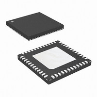
ISL6312IRZ Intersil, ISL6312IRZ Datasheet - Page 29

ISL6312IRZ
Manufacturer Part Number
ISL6312IRZ
Description
IC CTRLR PWM 4PHASE BUCK 48-QFN
Manufacturer
Intersil
Datasheet
1.ISL6312CRZ.pdf
(35 pages)
Specifications of ISL6312IRZ
Applications
Controller, Intel VR10, VR11, AMD CPU
Voltage - Input
5 ~ 12 V
Number Of Outputs
1
Voltage - Output
0.38 ~ 1.6 V
Operating Temperature
-40°C ~ 85°C
Mounting Type
Surface Mount
Package / Case
48-VQFN
Lead Free Status / RoHS Status
Lead free / RoHS Compliant
Loadline Regulation Resistor
If loadline regulation is desired, the IDROOP pin should be
shorted to the FB pin in order for the internal average
sense current to flow out across the loadline regulation
resistor, labeled R
the desired loadline required for the application. The
desired loadline, R
where V
current I
Based on the desired loadline, the loadline regulation
resistor, R
Equation 40, depending on the R-C current sense circuitry
being employed. If a basic R-C sense circuit consisting of C1
and R1 is being used, use Equation 39. If a resistor divider
R-C sense circuit consisting of R1, R2, and C1 is being
used, use Equation 40.
In Equations 39 and 40, R
the number of active channels; DCR is the DCR of the
individual output inductors; and R1 and R2 are the current
sense R-C resistors.
If no loadline regulation is required, the IDROOP pin should
be left open and not connected to anything. To choose the
value for R
“COMPENSATION WITHOUT LOAD-LINE REGULATION”
on page 30.
Compensation
The two opposing goals of compensating the voltage
regulator are stability and speed. Depending on whether the
regulator employs the optional load-line regulation as
described in Load-Line Regulation, there are two distinct
methods for achieving these goals.
R
R
R
3. Select new values, R
4. Replace R
LL
FB
FB
constant resistors based on the original values, R
and R
that the error is corrected. Repeat the procedure if
necessary.
R
R
=
=
=
1 NEW
2 NEW
,
,
V
------------------------ -
R
--------------------------------- -
R
----------------------------------------------------------------
DROOP
FL
DROOP
LL
LL
2,OLD
I
FB
.
FL
FB
DCR
⋅
⋅
, can be calculated from Equation 39 or
=
=
N 300
N 300
in this situation, please refer to the
DCR R
1
⋅
⋅
R
R
, using Equations 36 and 37.
and R
is the desired droop voltage at the full load
1 OLD
2 OLD
,
,
FB
LL
⋅
⋅
(
, can be calculated by Equation 38
R
2
in Figure 6. This resistor’s value sets
2
⋅
⋅
1
with the new values and check to see
Δ
----------
Δ
Δ
----------
Δ
+
1,NEW
V
V
V
V
R
LL
1
2
1
2
2
29
)
is the loadline resistance; N is
and R
2,NEW
, for the time
(EQ. 38)
(EQ. 39)
(EQ. 40)
(EQ. 36)
(EQ. 37)
1,OLD
ISL6312
COMPENSATION WITH LOAD-LINE REGULATION
The load-line regulated converter behaves in a similar
manner to a peak current mode controller because the two
poles at the output filter L-C resonant frequency split with the
introduction of current information into the control loop. The
final location of these poles is determined by the system
function, the gain of the current signal, and the value of the
compensation components, R
Since the system poles and zero are affected by the values
of the components that are meant to compensate them, the
solution to the system equation becomes fairly complicated.
Fortunately, there is a simple approximation that comes very
close to an optimal solution. Treating the system as though it
were a voltage-mode regulator, by compensating the L-C
poles and the ESR zero of the voltage mode approximation,
yields a solution that is always stable with very close to ideal
transient performance.
Select a target bandwidth for the compensated system, f0.
The target bandwidth must be large enough to assure
adequate transient performance, but smaller than 1/3 of the
per-channel switching frequency. The values of the
compensation components depend on the relationships of f0
to the L-C pole frequency and the ESR zero frequency. For
each of the following three, there is a separate set of
equations for the compensation components.
In Equation 41, L is the per-channel filter inductance divided
by the number of active channels; C is the sum total of all
output capacitors; ESR is the equivalent series resistance of
the bulk output filter capacitance; and V
peak-to-peak sawtooth signal amplitude as described in the
“Electrical Specifications” on page 6.
Once selected, the compensation values in Equation 41
assure a stable converter with reasonable transient
performance. In most cases, transient performance can be
improved by making adjustments to RC. Slowly increase the
value of RC while observing the transient performance on an
oscilloscope until no further improvement is noted. Normally,
CC will not need adjustment. Keep the value of CC from
Equation 41 unless some performance issue is noted.
FIGURE 20. COMPENSATION CONFIGURATION FOR
R
FB
LOAD-LINE REGULATED ISL6312 CIRCUIT
R
C
C
2
C
(OPTIONAL)
C
C
and C
IDROOP
COMP
VDIFF
FB
C
.
PP
is the
ISL6312
February 1, 2011
FN9289.6


