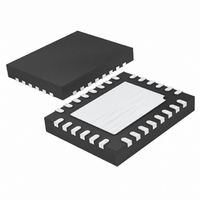
LTC3850EUF#PBF Linear Technology, LTC3850EUF#PBF Datasheet - Page 16

LTC3850EUF#PBF
Manufacturer Part Number
LTC3850EUF#PBF
Description
IC CNTRLR STP DWN SYNC 28-QFN
Manufacturer
Linear Technology
Series
PolyPhase®r
Type
Step-Down (Buck)r
Datasheet
1.LTC3850EUFPBF.pdf
(38 pages)
Specifications of LTC3850EUF#PBF
Internal Switch(s)
No
Synchronous Rectifier
Yes
Number Of Outputs
2
Voltage - Output
0.8 ~ 23.3 V
Current - Output
100mA
Frequency - Switching
250kHz ~ 780kHz
Voltage - Input
4 ~ 24 V
Operating Temperature
-40°C ~ 85°C
Mounting Type
Surface Mount
Package / Case
28-QFN
Primary Input Voltage
24V
No. Of Outputs
2
Output Current
100mA
No. Of Pins
28
Operating Temperature Range
-40°C To +85°C
Msl
MSL 1 - Unlimited
Supply Voltage Range
4V To 24V
Rohs Compliant
Yes
Lead Free Status / RoHS Status
Lead free / RoHS Compliant
Power - Output
-
Available stocks
Company
Part Number
Manufacturer
Quantity
Price
LTC3850/LTC3850-1
APPLICATIONS INFORMATION
Ensure that R1 has a power rating higher than this value.
If high efficiency is necessary at light loads, consider this
power loss when deciding whether to use DCR sensing or
sense resistors. Light load power loss can be modestly
higher with a DCR network than with a sense resistor,
due to the extra switching losses incurred through R1.
However, DCR sensing eliminates a sense resistor, re-
duces conduction losses and provides higher efficiency
at heavy loads. Peak efficiency is about the same with
either method.
To maintain a good signal to noise ratio for the current
sense signal, use a minimum ∆V
For a DCR sensing application, the actual ripple voltage
will be determined by the equation:
Slope Compensation and Inductor Peak Current
Slope compensation provides stability in constant-
frequency architectures by preventing subharmonic
oscillations at high duty cycles. It is accomplished inter-
nally by adding a compensating ramp to the inductor
current signal at duty cycles in excess of 40%. Normally,
this results in a reduction of maximum inductor peak cur-
rent for duty cycles > 40%. However, the LTC3850 uses
a patented scheme that counteracts this compensating
ramp, which allows the maximum inductor peak current
to remain unaffected throughout all duty cycles.
Inductor Value Calculation
Given the desired input and output voltages, the inductor
value and operating frequency f
inductor’s peak-to-peak ripple current:
Lower ripple current reduces core losses in the inductor,
ESR losses in the output capacitors, and output voltage
ripple. Thus, highest efficiency operation is obtained at
low frequency with a small ripple current. Achieving this,
however, requires a large inductor.
16
I
∆V
RIPPLE
SENSE
=
=
V
V
OUT
V
IN
IN
R1• C1
− V
V
IN
OUT
f
OSC
– V
V
• L
OUT
IN
V
OUT
• f
OSC
OSC
SENSE
directly determine the
of 10mV to 15mV.
A reasonable starting point is to choose a ripple current
that is about 40% of I
current occurs at the highest input voltage. To guarantee
that ripple current does not exceed a specified maximum,
the inductor should be chosen according to:
Inductor Core Selection
Once the inductance value is determined, the type of in-
ductor must be selected. Core loss is independent of core
size for a fixed inductor value, but it is very dependent
on inductance selected. As inductance increases, core
losses go down. Unfortunately, increased inductance
requires more turns of wire and therefore copper losses
will increase.
Ferrite designs have very low core loss and are preferred
at high switching frequencies, so design goals can con-
centrate on copper loss and preventing saturation. Ferrite
core material saturates “hard,” which means that induc-
tance collapses abruptly when the peak design current is
exceeded. This results in an abrupt increase in inductor
ripple current and consequent output voltage ripple. Do
not allow the core to saturate!
Power MOSFET and Schottky Diode
(Optional) Selection
Two external power MOSFETs must be selected for each
controller in the LTC3850: one N-channel MOSFET for the
top (main) switch, and one N-channel MOSFET for the
bottom (synchronous) switch.
The peak-to-peak drive levels are set by the INTV
voltage. This voltage is typically 5V during start-up
(see EXTV
threshold MOSFETs must be used in most applications.
The only exception is if low input voltage is expected (V
< 5V); then, sub-logic level threshold MOSFETs (V
< 3V) should be used. Pay close attention to the BV
specification for the MOSFETs as well; most of the logic
level MOSFETs are limited to 30V or less.
Selection criteria for the power MOSFETs include the
on-resistance R
L ≥
f
OSC
V
IN
CC
– V
•I
RIPPLE
Pin Connection). Consequently, logic-level
OUT
DS(ON)
•
OUT(MAX)
V
, Miller capacitance C
V
OUT
IN
. Note that the largest ripple
MILLER
, input
GS(TH)
38501fc
DSS
CC
IN


