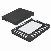
LTC3850EUF#PBF Linear Technology, LTC3850EUF#PBF Datasheet - Page 22

LTC3850EUF#PBF
Manufacturer Part Number
LTC3850EUF#PBF
Description
IC CNTRLR STP DWN SYNC 28-QFN
Manufacturer
Linear Technology
Series
PolyPhase®r
Type
Step-Down (Buck)r
Datasheet
1.LTC3850EUFPBF.pdf
(38 pages)
Specifications of LTC3850EUF#PBF
Internal Switch(s)
No
Synchronous Rectifier
Yes
Number Of Outputs
2
Voltage - Output
0.8 ~ 23.3 V
Current - Output
100mA
Frequency - Switching
250kHz ~ 780kHz
Voltage - Input
4 ~ 24 V
Operating Temperature
-40°C ~ 85°C
Mounting Type
Surface Mount
Package / Case
28-QFN
Primary Input Voltage
24V
No. Of Outputs
2
Output Current
100mA
No. Of Pins
28
Operating Temperature Range
-40°C To +85°C
Msl
MSL 1 - Unlimited
Supply Voltage Range
4V To 24V
Rohs Compliant
Yes
Lead Free Status / RoHS Status
Lead free / RoHS Compliant
Power - Output
-
Available stocks
Company
Part Number
Manufacturer
Quantity
Price
LTC3850/LTC3850-1
APPLICATIONS INFORMATION
suggested. A 2.2Ω – 10Ω resistor placed between C
(C1) and the V
the two channels.
The selection of C
resistance (ESR). Typically, once the ESR requirement
is satisfied, the capacitance is adequate for filtering. The
output ripple (∆V
where f is the operating frequency, C
capacitance and I
tor. The output ripple is highest at maximum input voltage
since I
Setting Output Voltage
The LTC3850 output voltages are each set by an external
feedback resistive divider carefully placed across the out-
put, as shown in Figure 9. The regulated output voltage
is determined by:
To improve the frequency response, a feed-forward ca-
pacitor, C
route the V
inductor or the SW line.
Fault Conditions: Current Limit and Current Foldback
The LTC3850 includes current foldback to help limit load
current when the output is shorted to ground. If the out-
put falls below 50% of its nominal output level, then the
maximum sense voltage is progressively lowered from its
maximum programmed value to one-third of the maximum
value. Foldback current limiting is disabled during the
22
∆V
V
OUT
OUT
RIPPLE
= 0.8V • 1+
FF
≈I
, may be used. Great care should be taken to
FB
RIPPLE
increases with input voltage.
line away from noise sources, such as the
Figure 9. Setting Output Voltage
IN
1/2 LTC3850
OUT
RIPPLE
pin provides further isolation between
OUT
) is approximated by:
ESR +
V
R
R
FB
is driven by the effective series
B
A
is the ripple current in the induc-
8fC
V
OUT
1
OUT
R
R
38501 F09
B
A
C
OUT
FF
is the output
IN
soft-start or tracking up. Under short-circuit conditions
with very low duty cycles, the LTC3850 will begin cycle
skipping in order to limit the short-circuit current. In this
situation the bottom MOSFET will be dissipating most of
the power but less than in normal operation. The short-
circuit ripple current is determined by the minimum on-
time t
and inductor value:
The resulting short-circuit current is:
Phase-Locked Loop and Frequency Synchronization
The LTC3850 has a phase-locked loop (PLL) comprised of
an internal voltage-controlled oscillator (V
detector. This allows the turn-on of the top MOSFET of
controller 1 to be locked to the rising edge of an external
clock signal applied to the MODE/PLLIN pin. The turn-on
of controller 2’s top MOSFET is thus 180 degrees out-
of-phase with the external clock. The phase detector is
an edge sensitive digital type that provides zero degrees
phase shift between the external and internal oscillators.
This type of phase detector does not exhibit false lock to
harmonics of the external clock.
The output of the phase detector is a pair of complemen-
tary current sources that charge or discharge the external
filter network connected to the FREQ/PLLFLTR pin. The
relationship between the voltage on the FREQ/PLLFLTR
pin and operating frequency is shown in Figure 10 and
specified in the Electrical Characteristics table. Note that
the LTC3850 can only be synchronized to an external clock
whose frequency is within range of the LTC3850’s internal
V
A simplified block diagram is shown in Figure 11.
If no clock is applied to MODE/PLLIN pin, the FREQ/
PLLFLTR pin will be high impedance.
If the external clock frequency is greater than the internal
oscillator’s frequency, f
CO
I
∆I
SC
. This is guaranteed to be between 250kHz and 780kHz.
L(SC)
ON(MIN)
=
1/3 V
= t
R
ON(MIN)
of the LTC3850 (≈ 90ns), the input voltage
SENSE(MAX)
SENSE
•
V
OSC
L
IN
–
, then current is sourced con-
2
1
∆I
L(SC)
CO
) and a phase
38501fc


