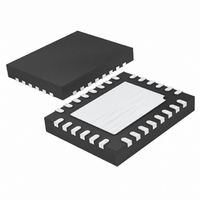
LTC3850EUF#PBF Linear Technology, LTC3850EUF#PBF Datasheet - Page 29

LTC3850EUF#PBF
Manufacturer Part Number
LTC3850EUF#PBF
Description
IC CNTRLR STP DWN SYNC 28-QFN
Manufacturer
Linear Technology
Series
PolyPhase®r
Type
Step-Down (Buck)r
Datasheet
1.LTC3850EUFPBF.pdf
(38 pages)
Specifications of LTC3850EUF#PBF
Internal Switch(s)
No
Synchronous Rectifier
Yes
Number Of Outputs
2
Voltage - Output
0.8 ~ 23.3 V
Current - Output
100mA
Frequency - Switching
250kHz ~ 780kHz
Voltage - Input
4 ~ 24 V
Operating Temperature
-40°C ~ 85°C
Mounting Type
Surface Mount
Package / Case
28-QFN
Primary Input Voltage
24V
No. Of Outputs
2
Output Current
100mA
No. Of Pins
28
Operating Temperature Range
-40°C To +85°C
Msl
MSL 1 - Unlimited
Supply Voltage Range
4V To 24V
Rohs Compliant
Yes
Lead Free Status / RoHS Status
Lead free / RoHS Compliant
Power - Output
-
Available stocks
Company
Part Number
Manufacturer
Quantity
Price
APPLICATIONS INFORMATION
The Coiltronics (Cooper) HCP0703-2R2 (20mΩ DCR
at 20°C) and HCP0703-3R3 (30mΩ DCR
chosen. At 100°C, the estimated maximum DCR values are
26.4mΩ and 39.6mΩ. The divider ratios are:
For each channel, 0.1µF is selected for C1.
For channel 1, the DCR
The power loss in R1 at the maximum input voltage is:
R
R1||R2 =
R1=
R2 =
P
and
= 1.1k ; and
(20V − 3.3V) • 3.3V
LOSS
D
=
R1||R2
R1 • R
DCR
Figure 15. Design Example Efficiency vs Load
1− R
R1=
39.6mΩ
R
100
6.19k
90
80
70
60
50
40
R
7mΩ
D
0.01
(DCR
SENSE(EQUIV)
MAX
D
(V
D
=
IN(MAX)
=
MAX
0.18
at T
1.1k
6.19k • 0.18
≅ 0.18
30mΩ • 0.1µF
1− 0.18
LOAD CURRENT (mA)
L(MAX)
0.1
at 20°C) • C1
L
3.3µH
SENSE
≅ 6.19k;
− V
= 9mW
R1
OUT
=
filter/divider values are:
) • V
26.4mΩ
≅ 1.33k
1
7mΩ
EFFICIENCY
POWER LOSS
7mΩ
= 1.1k
OUT
=
20mΩ • 0.1µF
DCR
=
DCR
38501 F15
MAX
= 0.26;
10
2.2µH
10
1
0.1
0.01
at 20°C) are
MAX
The respective values for Channel 2 are R1 = 4.12k, R2 =
1.5k; and P
Burst Mode operation is chosen for high light load efficiency
(Figure 15) by floating the MODE/PLLIN pin. Power loss
due to the DCR sensing network is slightly higher at light
loads than would have been the case with a suitable sense
resistor (7mΩ). At heavier loads, DCR sensing provides
higher efficiency.
The power dissipation on the topside MOSFET can be easily
estimated. Choosing a Siliconix Si4816BDY dual MOSFET
results in: R
At maximum input voltage with T(estimated) = 50°C:
A short-circuit to ground will result in a folded back cur-
rent of:
with a typical value of R
= 0.1. The resulting power dissipated in the bottom
MOSFET is:
which is less than under full-load conditions.
C
temperature assuming only channel 1 or 2 is on. C
chosen with an ESR of 0.02Ω for low output ripple. The
output ripple in continuous mode will be highest at the
maximum input voltage. The output voltage ripple due to
ESR is approximately:
IN
V
P
I
P
(
SC
is chosen for an RMS current rating of at least 2A at
0.023Ω
MAIN
SYNC
ORIPPLE
5 – 2.3
=
1
(
=
1/ 3
=
= 66mW
0.007Ω
LOSS
3.3V
20V – 3.3V
20V
+
)
= R
DS(ON)
+ 20V
)
2.3
50mV
(
1
20V
ESR
LTC3850/LTC3850-1
R1 = 8mW.
( )
5
500kHz
(
= 0.023Ω/0.016Ω, C
(∆I
2
)
[
–
2
1+ (0.005)(50°C – 25°C)
L
2
1
(
) = 0.02Ω(1.5A) = 30mV
5A
2.1A
DS(ON)
2
90ns(20V)
)
= 186mW
3.3µH
( )
)
2Ω
2
(
and d = (0.005/°C)(20)
1.125
(
100pF
)
(
= 2.1A
MILLER
0.016Ω
)
•
]
@ 100pF .
P–P
•
)
29
OUT
38501fc
is


