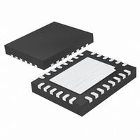
LTC3850EUF#PBF Linear Technology, LTC3850EUF#PBF Datasheet - Page 20

LTC3850EUF#PBF
Manufacturer Part Number
LTC3850EUF#PBF
Description
IC CNTRLR STP DWN SYNC 28-QFN
Manufacturer
Linear Technology
Series
PolyPhase®r
Type
Step-Down (Buck)r
Datasheet
1.LTC3850EUFPBF.pdf
(38 pages)
Specifications of LTC3850EUF#PBF
Internal Switch(s)
No
Synchronous Rectifier
Yes
Number Of Outputs
2
Voltage - Output
0.8 ~ 23.3 V
Current - Output
100mA
Frequency - Switching
250kHz ~ 780kHz
Voltage - Input
4 ~ 24 V
Operating Temperature
-40°C ~ 85°C
Mounting Type
Surface Mount
Package / Case
28-QFN
Primary Input Voltage
24V
No. Of Outputs
2
Output Current
100mA
No. Of Pins
28
Operating Temperature Range
-40°C To +85°C
Msl
MSL 1 - Unlimited
Supply Voltage Range
4V To 24V
Rohs Compliant
Yes
Lead Free Status / RoHS Status
Lead free / RoHS Compliant
Power - Output
-
Available stocks
Company
Part Number
Manufacturer
Quantity
Price
LTC3850/LTC3850-1
APPLICATIONS INFORMATION
exceeded. The INTV
gate charge current, may be supplied by either the 5V linear
regulator or EXTV
is less than 4.7V, the linear regulator is enabled. Power
dissipation for the IC in this case is highest and is equal
to V
on operating frequency as discussed in the Efficiency
Considerations section. The junction temperature can be
estimated by using the equations given in Note 3 of the
Electrical Characteristics. For example, the LTC3850 INTV
current is limited to less than 24mA from a 24V supply in
the GN package and not using the EXTV
To prevent the maximum junction temperature from being
exceeded, the input supply current must be checked while
operating in continuous conduction mode (MODE/PLLIN =
SGND) at maximum V
rises above 4.7V, the INTV
and the EXTV
remains on as long as the voltage applied to EXTV
above 4.5V. Using the EXTV
and control power to be derived from one of the LTC3850’s
switching regulator outputs during normal operation and
from the INTV
(e.g., start-up, short-circuit). If more current is required
through the EXTV
diode can be added between the EXTV
Do not apply more than 6V to the EXTV
sure that EXTV
Significant efficiency and thermal gains can be realized by
powering INTV
resulting from the driver and control currents will be scaled
by a factor of (Duty Cycle)/(Switcher Efficiency).
Tying the EXTV
temperature in the previous example from 125°C to:
However, for 3.3V and other low voltage outputs, addi-
tional circuitry is required to derive INTV
the output.
The following list summarizes the four possible connec-
tions for EXTV
20
T
T
J
J
IN
= 70°C + (24mA)(24V)(95°C/W) = 125°C
= 70°C + (24mA)(5V)(95°C/W) = 81°C
• I
INTVCC
CC
CC
CC
CC
CC
CC
. The gate charge current is dependent
is connected to the INTV
:
CC
CC
< V
pin to a 5V supply reduces the junction
from the output, since the V
when the output is out of regulation
CC
. When the voltage on the EXTV
than is specified, an external Schottky
IN
IN
current, which is dominated by the
. When the voltage applied to EXTV
.
CC
CC
linear regulator is turned off
allows the MOSFET driver
CC
CC
and INTV
CC
CC
CC
supply:
pin and make
. The EXTV
power from
CC
IN
remains
CC
current
CC
pins.
pin
CC
CC
CC
Topside MOSFET Driver Supply (C
External bootstrap capacitors C
pins supply the gate drive voltages for the topside MOSFETs.
Capacitor C
external diode DB from INTV
When one of the topside MOSFETs is to be turned on,
the driver places the C
of the desired MOSFET. This enhances the MOSFET and
1. EXTV
2. EXTV
3. EXTV
4. EXTV
For applications where the main input power is 5V, tie
the V
pins to the 5V input with a 1Ω or 2.2Ω resistor as shown
in Figure 8 to minimize the voltage drop caused by the
gate charge current. This will override the INTV
regulator and will prevent INTV
due to the dropout voltage. Make sure the INTV
is at or exceeds the R
which is typically 4.5V for logic level devices.
INTV
resulting in an efficiency penalty of up to 10% at high
input voltages.
normal connection for a 5V regulator and provides
the highest efficiency.
external supply is available, it may be used to power
EXTV
gate drive requirements.
work. For 3.3V and other low voltage regulators,
efficiency gains can still be realized by connecting
EXTV
boosted to greater than 4.7V.
IN
CC
and INTV
CC
CC
CC
CC
CC
CC
to be powered from the internal 5V regulator
B
providing it is compatible with the MOSFET
connected to an output-derived boost net-
to an output-derived voltage that has been
connected to an external supply. If a 5V
left open (or grounded). This will cause
connected directly to V
in the Functional Diagram is charged though
LTC3850
Figure 8. Setup for a 5V Input
CC
INTV
pins together and tie the combined
V
DS(ON)
CC
IN
B
voltage across the gate source
CINTV
test voltage for the MOSFET
CC
4.7µF
B
CC
CC
when the SW pin is low.
connected to the BOOST
from dropping too low
R
B
1Ω
VIN
, DB)
OUT
+
38501 F08
. This is the
C
5V
IN
CC
CC
voltage
linear
38501fc


