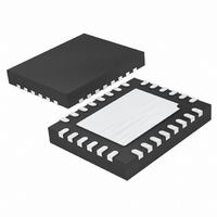
LTC3850EUF#PBF Linear Technology, LTC3850EUF#PBF Datasheet - Page 25

LTC3850EUF#PBF
Manufacturer Part Number
LTC3850EUF#PBF
Description
IC CNTRLR STP DWN SYNC 28-QFN
Manufacturer
Linear Technology
Series
PolyPhase®r
Type
Step-Down (Buck)r
Datasheet
1.LTC3850EUFPBF.pdf
(38 pages)
Specifications of LTC3850EUF#PBF
Internal Switch(s)
No
Synchronous Rectifier
Yes
Number Of Outputs
2
Voltage - Output
0.8 ~ 23.3 V
Current - Output
100mA
Frequency - Switching
250kHz ~ 780kHz
Voltage - Input
4 ~ 24 V
Operating Temperature
-40°C ~ 85°C
Mounting Type
Surface Mount
Package / Case
28-QFN
Primary Input Voltage
24V
No. Of Outputs
2
Output Current
100mA
No. Of Pins
28
Operating Temperature Range
-40°C To +85°C
Msl
MSL 1 - Unlimited
Supply Voltage Range
4V To 24V
Rohs Compliant
Yes
Lead Free Status / RoHS Status
Lead free / RoHS Compliant
Power - Output
-
Available stocks
Company
Part Number
Manufacturer
Quantity
Price
APPLICATIONS INFORMATION
pin. The bandwidth can also be estimated by examining the
rise time at the pin. The I
in the Typical Application circuit will provide an adequate
starting point for most applications.
The I
loop compensation. The values can be modified slightly
(from 0.5 to 2 times their suggested values) to optimize
transient response once the final PC layout is done and
the particular output capacitor type and value have been
determined. The output capacitors need to be selected
because the various types and values determine the loop
gain and phase. An output current pulse of 20% to 80%
of full-load current having a rise time of 1µs to 10µs will
produce output voltage and I
give a sense of the overall loop stability without break-
ing the feedback loop. Placing a power MOSFET directly
across the output capacitor and driving the gate with an
appropriate signal generator is a practical way to produce
a realistic load step condition. The initial output voltage
step resulting from the step change in output current may
not be within the bandwidth of the feedback loop, so this
signal cannot be used to determine phase margin. This
is why it is better to look at the I
the feedback loop and is the filtered and compensated
control loop response. The gain of the loop will be in-
creased by increasing R
will be increased by decreasing C
the same factor that C
will be kept the same, thereby keeping the phase shift the
same in the most critical frequency range of the feedback
loop. The output voltage settling behavior is related to the
stability of the closed-loop system and will demonstrate
the actual overall supply performance.
A second, more severe transient is caused by switching
in loads with large (>1µF) supply bypass capacitors. The
discharged bypass capacitors are effectively put in parallel
with C
alter its delivery of current quickly enough to prevent this
sudden step change in output voltage if the load switch
resistance is low and it is driven quickly. If the ratio of
C
should be controlled so that the load rise time is limited
LOAD
TH
OUT
to C
series R
, causing a rapid drop in V
OUT
is greater than 1:50, the switch rise time
C
-C
C
filter sets the dominant pole-zero
C
is decreased, the zero frequency
C
TH
and the bandwidth of the loop
external components shown
TH
TH
pin waveforms that will
C
. If R
pin signal which is in
OUT
. No regulator can
C
is increased by
to approximately 25 • C
require a 250µs rise time, limiting the charging current
to about 200mA.
PC Board Layout Checklist
When laying out the printed circuit board, the following
checklist should be used to ensure proper operation of
the IC. These items are also illustrated graphically in the
layout diagram of Figure 12. Figure 13 illustrates the
current waveforms present in the various branches of
the 2-phase synchronous regulators operating in the
continuous mode. Check the following in your layout:
1. Are the top N-channel MOSFETs M1 and M3 located
2. Are the signal and power grounds kept separate? The
3. Do the LTC3850 V
4. Are the SENSE
within 1 cm of each other with a common drain con-
nection at C
decoupling for the two channels as it can cause a large
resonant loop.
combined IC signal ground pin and the ground return
of C
minals. The V
possible. The path formed by the top N-channel MOSFET,
Schottky diode and the C
leads and PC trace lengths. The output capacitor (–)
terminals should be connected as close as possible
to the (–) terminals of the input capacitor by placing
the capacitors next to each other and away from the
Schottky loop described above.
the (+) terminals of C
connected between the (+) terminal of C
ground. The feedback resistor connections should not
be along the high current input feeds from the input
capacitor(s).
minimum PC trace spacing? The filter capacitor between
SENSE
to the IC. Ensure accurate current sensing with Kelvin
connections at the sense resistor or inductor, whichever
is used for current sensing.
INTVCC
+
and SENSE
must return to the combined C
IN
LTC3850/LTC3850-1
FB
+
? Do not attempt to split the input
and SENSE
and I
FB
LOAD
–
pins’ resistive dividers connect to
OUT
TH
should be as close as possible
? The resistive divider must be
IN
. Thus a 10µF capacitor would
traces should be as short as
capacitor should have short
–
leads routed together with
OUT
OUT
and signal
25
(–) ter-
38501fc


