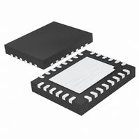
LTC3850EUF#PBF Linear Technology, LTC3850EUF#PBF Datasheet - Page 21

LTC3850EUF#PBF
Manufacturer Part Number
LTC3850EUF#PBF
Description
IC CNTRLR STP DWN SYNC 28-QFN
Manufacturer
Linear Technology
Series
PolyPhase®r
Type
Step-Down (Buck)r
Datasheet
1.LTC3850EUFPBF.pdf
(38 pages)
Specifications of LTC3850EUF#PBF
Internal Switch(s)
No
Synchronous Rectifier
Yes
Number Of Outputs
2
Voltage - Output
0.8 ~ 23.3 V
Current - Output
100mA
Frequency - Switching
250kHz ~ 780kHz
Voltage - Input
4 ~ 24 V
Operating Temperature
-40°C ~ 85°C
Mounting Type
Surface Mount
Package / Case
28-QFN
Primary Input Voltage
24V
No. Of Outputs
2
Output Current
100mA
No. Of Pins
28
Operating Temperature Range
-40°C To +85°C
Msl
MSL 1 - Unlimited
Supply Voltage Range
4V To 24V
Rohs Compliant
Yes
Lead Free Status / RoHS Status
Lead free / RoHS Compliant
Power - Output
-
Available stocks
Company
Part Number
Manufacturer
Quantity
Price
APPLICATIONS INFORMATION
turns on the topside switch. The switch node voltage, SW,
rises to V
MOSFET on, the boost voltage is above the input supply:
V
C
citance of the topside MOSFET(s). The reverse break-
down of the external Schottky diode must be greater
than V
final arbiter is the total input current for the regulator. If
a change is made and the input current decreases, then
the efficiency has improved. If there is no change in input
current, then there is no change in efficiency.
Undervoltage Lockout
The LTC3850 has two functions that help protect the
controller in case of undervoltage conditions. A precision
UVLO comparator constantly monitors the INTV
to ensure that an adequate gate-drive voltage is present.
It locks out the switching action when INTV
3V. To prevent oscillation when there is a disturbance on
the INTV
sion hysteresis.
Another way to detect an undervoltage condition is to
monitor the V
precision turn-on reference of 1.2V, one can use a resistor
divider to V
An extra 4.5µA of current flows out of the RUN pin once
the RUN pin voltage passes 1.2V. One can program the
hysteresis of the run comparator by adjusting the values
of the resistive divider. For accurate V
detection, V
C
The selection of C
ture and its impact on the worst-case RMS current drawn
through the input network (battery/fuse/capacitor). It can
be shown that the worst-case capacitor RMS current occurs
when only one controller is operating. The controller with
the highest (V
formula below to determine the maximum RMS capacitor
current requirement. Increasing the output current drawn
from the other controller will actually decrease the input
RMS ripple current from its maximum value. The out-of-
phase technique typically reduces the input capacitor’s RMS
BOOST
B
IN
needs to be 100 times that of the total input capa-
and C
IN(MAX)
= V
CC
IN
OUT
IN
, the UVLO comparator has 500mV of preci-
IN
and the BOOST pin follows. With the topside
IN
+ V
. When adjusting the gate drive level, the
to turn on the IC when V
Selection
OUT
IN
needs to be higher than 4V.
INTVCC
supply. Because the RUN pins have a
)(I
IN
is simplified by the 2-phase architec-
OUT
. The value of the boost capacitor
) product needs to be used in the
IN
IN
is high enough.
undervoltage
CC
CC
is below
voltage
ripple current by a factor of 30% to 70% when compared
to a single phase power supply solution.
In continuous mode, the source current of the top MOSFET
is a square wave of duty cycle (V
large voltage transients, a low ESR capacitor sized for the
maximum RMS current of one channel must be used. The
maximum RMS capacitor current is given by:
This formula has a maximum at V
= I
used for design because even significant deviations do not
offer much relief. Note that capacitor manufacturers’ ripple
current ratings are often based on only 2000 hours of life.
This makes it advisable to further derate the capacitor, or
to choose a capacitor rated at a higher temperature than
required. Several capacitors may be paralleled to meet
size or height requirements in the design. Due to the high
operating frequency of the LTC3850, ceramic capacitors
can also be used for C
if there is any question.
The benefit of the LTC3850 2-phase operation can be cal-
culated by using the equation above for the higher power
controller and then calculating the loss that would have
resulted if both controller channels switched on at the same
time. The total RMS power lost is lower when both control-
lers are operating due to the reduced overlap of current
pulses required through the input capacitor’s ESR. This is
why the input capacitor’s requirement calculated above for
the worst-case controller is adequate for the dual controller
design. Also, the input protection fuse resistance, battery
resistance, and PC board trace resistance losses are also
reduced due to the reduced peak currents in a 2-phase
system. The overall benefit of a multiphase design will
only be fully realized when the source impedance of the
power supply/battery is included in the efficiency testing.
The sources of the top MOSFETs should be placed within
1cm of each other and share a common C
the sources and C
current resonances at V
A small (0.1µF to 1µF) bypass capacitor between the chip
V
IN
OUT
C
pin and ground, placed close to the LTC3850, is also
IN
/2. This simple worst-case condition is commonly
Required I
LTC3850/LTC3850-1
IN
RMS
may produce undesirable voltage and
IN
≈
. Always consult the manufacturer
IN
I
MAX
V
.
IN
(
V
OUT
IN
OUT
= 2V
)
)/(V
(
V
IN
IN
OUT
IN
(s). Separating
– V
). To prevent
, where I
OUT
21
)
38501fc
1/2
RMS


