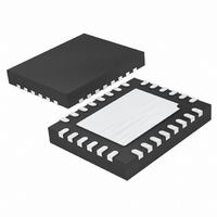
LTC3850EUF#PBF Linear Technology, LTC3850EUF#PBF Datasheet - Page 23

LTC3850EUF#PBF
Manufacturer Part Number
LTC3850EUF#PBF
Description
IC CNTRLR STP DWN SYNC 28-QFN
Manufacturer
Linear Technology
Series
PolyPhase®r
Type
Step-Down (Buck)r
Datasheet
1.LTC3850EUFPBF.pdf
(38 pages)
Specifications of LTC3850EUF#PBF
Internal Switch(s)
No
Synchronous Rectifier
Yes
Number Of Outputs
2
Voltage - Output
0.8 ~ 23.3 V
Current - Output
100mA
Frequency - Switching
250kHz ~ 780kHz
Voltage - Input
4 ~ 24 V
Operating Temperature
-40°C ~ 85°C
Mounting Type
Surface Mount
Package / Case
28-QFN
Primary Input Voltage
24V
No. Of Outputs
2
Output Current
100mA
No. Of Pins
28
Operating Temperature Range
-40°C To +85°C
Msl
MSL 1 - Unlimited
Supply Voltage Range
4V To 24V
Rohs Compliant
Yes
Lead Free Status / RoHS Status
Lead free / RoHS Compliant
Power - Output
-
Available stocks
Company
Part Number
Manufacturer
Quantity
Price
APPLICATIONS INFORMATION
tinuously from the phase detector output, pulling up the
FREQ/PLLFLTR pin. When the external clock frequency
is less than f
down the FREQ/PLLFLTR pin. If the external and internal
frequencies are the same but exhibit a phase difference,
the current sources turn on for an amount of time corre-
sponding to the phase difference. The voltage on the FREQ/
PLLFLTR pin is adjusted until the phase and frequency of
the internal and external oscillators are identical. At the
stable operating point, the phase detector output is high
impedance and the filter capacitor C
The loop filter components, C
current pulses from the phase detector and provide a
stable input to the voltage-controlled oscillator. The filter
components C
acquires lock. Typically R
0.01µF .
OSCILLATOR
EXTERNAL
Figure 10. Relationship Between Oscillator
Frequency and Voltage at the FREQ/PLLFLTR Pin
Figure 11. Phase-Locked Loop Block Diagram
900
800
700
600
500
400
300
200
100
MODE/
PLLIN
0
0
OSC
LP
, current is sunk continuously, pulling
FREQ/PLLFLTR PIN VOLTAGE (V)
and R
FREQUENCY
0.5
DETECTOR
DIGITAL
PHASE/
LP
1
LP
determine how fast the loop
= 10k and C
LP
1.5
and R
2.4V
LP
2
LP
holds the voltage.
, smooth out the
38501 F10
LP
FREQ/
PLLFLTR
2.5
R
is 2200pF to
LP
VCO
38501 F11
C
LP
Typically, the external clock (on MODE/PLLIN pin)
input high threshold is 1.6V, while the input low thres-
hold is 1V.
Minimum On-Time Considerations
Minimum on-time t
that the LTC3850 is capable of turning on the top MOSFET.
It is determined by internal timing delays and the gate
charge required to turn on the top MOSFET. Low duty
cycle applications may approach this minimum on-time
limit and care should be taken to ensure that
If the duty cycle falls below what can be accommodated
by the minimum on-time, the controller will begin to skip
cycles. The output voltage will continue to be regulated,
but the ripple voltage and current will increase.
The minimum on-time for the LTC3850 is approximately
90ns, with reasonably good PCB layout, minimum 30%
inductor current ripple and at least 10mV – 15mV ripple
on the current sense signal. The minimum on-time can be
affected by PCB switching noise in the voltage and current
loop. As the peak sense voltage decreases the minimum
on-time gradually increases to 130ns. This is of particular
concern in forced continuous applications with low ripple
current at light loads. If the duty cycle drops below the
minimum on-time limit in this situation, a significant
amount of cycle skipping can occur with correspondingly
larger current and voltage ripple.
Efficiency Considerations
The percent efficiency of a switching regulator is equal to
the output power divided by the input power times 100%.
It is often useful to analyze individual losses to determine
what is limiting the efficiency and which change would
produce the most improvement. Percent efficiency can
be expressed as:
where L1, L2, etc. are the individual losses as a percent-
age of input power.
%Efficiency = 100% – (L1 + L2 + L3 + ...)
t
ON(MIN)
<
V
V
IN
OUT
LTC3850/LTC3850-1
(f)
ON(MIN)
is the smallest time duration
23
38501fc


