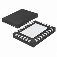
LTC3850EUF#PBF Linear Technology, LTC3850EUF#PBF Datasheet - Page 18

LTC3850EUF#PBF
Manufacturer Part Number
LTC3850EUF#PBF
Description
IC CNTRLR STP DWN SYNC 28-QFN
Manufacturer
Linear Technology
Series
PolyPhase®r
Type
Step-Down (Buck)r
Datasheet
1.LTC3850EUFPBF.pdf
(38 pages)
Specifications of LTC3850EUF#PBF
Internal Switch(s)
No
Synchronous Rectifier
Yes
Number Of Outputs
2
Voltage - Output
0.8 ~ 23.3 V
Current - Output
100mA
Frequency - Switching
250kHz ~ 780kHz
Voltage - Input
4 ~ 24 V
Operating Temperature
-40°C ~ 85°C
Mounting Type
Surface Mount
Package / Case
28-QFN
Primary Input Voltage
24V
No. Of Outputs
2
Output Current
100mA
No. Of Pins
28
Operating Temperature Range
-40°C To +85°C
Msl
MSL 1 - Unlimited
Supply Voltage Range
4V To 24V
Rohs Compliant
Yes
Lead Free Status / RoHS Status
Lead free / RoHS Compliant
Power - Output
-
Available stocks
Company
Part Number
Manufacturer
Quantity
Price
LTC3850/LTC3850-1
APPLICATIONS INFORMATION
selected mode once TK/SS > 0.74V. The output ripple is
minimized during the 100mV forced continuous mode
window ensuring a clean PGOOD signal.
When the channel is configured to track another supply,
the feedback voltage of the other supply is duplicated by
a resistor divider and applied to the TK/SS pin. Therefore,
the voltage ramp rate on this pin is determined by the
ramp rate of the other supply’s voltage. Note that the
small soft-start capacitor charging current is always
flowing, producing a small offset error. To minimize this
error, select the tracking resistive divider value to be small
enough to make this error negligible.
In order to track down another channel or supply after
the soft-start phase expires, the LTC3850 is forced into
continuous mode of operation as soon as V
undervoltage threshold of 0.74V regardless of the setting
on the MODE/PLLIN pin. However, the LTC3850 should
always be set in force continuous mode tracking down
when there is no load. After TK/SS drops below 0.1V, its
channel will operate in discontinuous mode.
Output Voltage Tracking
The LTC3850 allows the user to program how its out-
put ramps up and down by means of the TK/SS pins.
Through these pins, the output can be set up to ei-
ther coincidentally or ratiometrically track another
supply’s output, as shown in Figure 5. In the following
discussions, V
master channel and V
2 as a slave channel. In practice, though, either phase can
be used as the master. To implement the coincident track-
ing in Figure 5a, connect an additional resistive divider to
V
slave channel. The ratio of this divider should be the same
as that of the slave channel’s feedback divider shown in
Figure 6a. In this tracking mode, V
than V
of the V
master channel’s feedback divider. By selecting different
resistors, the LTC3850 can achieve different modes of
tracking including the two in Figure 5.
So which mode should be programmed? While either
mode in Figure 5 satisfies most practical applications,
18
OUT1
OUT2
and connect its midpoint to the TK/SS pin of the
OUT2
. To implement the ratiometric tracking, the ratio
divider should be exactly the same as the
OUT1
refers to the LTC3850’s output 1 as a
OUT2
refers to the LTC3850’s output
OUT1
must be set higher
FB
is below the
some tradeoffs exist. The ratiometric mode saves a pair
of resistors, but the coincident mode offers better output
regulation. This can be better understood with the help
of Figure 7. At the input stage of the slave channel’s error
amplifier, two common anode diodes are used to clamp
the equivalent reference voltage and an additional diode
is used to match the shifted common mode voltage. The
top two current sources are of the same amplitude. In the
coincident mode, the TK/SS voltage is substantially higher
than 0.8V at steady state and effectively turns off D1. D2
and D3 will therefore conduct the same current and offer
tight matching between V
0.8V reference. In the ratiometric mode, however, TK/SS
equals 0.8V at steady state. D1 will divert part of the bias
current to make V
Although this error is minimized by the exponential I-V
characteristic of the diode, it does impose a finite amount
of output voltage deviation. Furthermore, when the master
channel’s output experiences dynamic excursion (under
load transient, for example), the slave channel output will
be affected as well. For better output regulation, use the
coincident tracking mode instead of ratiometric.
INTV
The LTC3850 features an NPN linear regulator that supplies
power to INTV
gate drivers and much of the LTC3850’s internal circuitry.
The linear regulator regulates the voltage at the INTV
to 5V when V
INTV
needed power when its voltage is higher than 4.7V. Each
of these can supply a peak current of 100mA and must
be bypassed to ground with a minimum of 1µF ceramic
capacitor or low ESR electrolytic capacitor. No matter
what type of bulk capacitor is used, an additional 0.1µF
ceramic capacitor placed directly adjacent to the INTV
and PGND pins is highly recommended. Good bypassing
is needed to supply the high transient currents required
by the MOSFET gate drivers and to prevent interaction
between the channels.
High input voltage applications in which large MOSFETs
are being driven at high frequencies may cause the maxi-
mum junction temperature rating for the LTC3850 to be
CC
CC
through a P-channel MOSFET and can supply the
Regulators and EXTV
IN
CC
is greater than 6.5V. EXTV
from the V
FB2
slightly lower than 0.8V.
FB2
IN
CC
supply. INTV
and the internal precision
CC
CC
connects to
powers the
CC
38501fc
pin
CC


