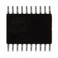
L6730TR STMicroelectronics, L6730TR Datasheet - Page 33

L6730TR
Manufacturer Part Number
L6730TR
Description
IC CTRLR ADJ STEP DOWN 20-TSSOP
Manufacturer
STMicroelectronics
Type
Step-Down (Buck)r
Datasheet
1.L6730TR.pdf
(52 pages)
Specifications of L6730TR
Internal Switch(s)
No
Synchronous Rectifier
Yes
Number Of Outputs
1
Voltage - Output
Adj to 0.6V
Frequency - Switching
100kHz ~ 1MHz
Voltage - Input
1.8 ~ 14 V
Operating Temperature
-40°C ~ 85°C
Mounting Type
Surface Mount
Package / Case
20-TSSOP Exposed Pad, 20-eTSSOP, 20-HTSSOP
Output Voltage
0.6 V
Input Voltage
1.8 V to 14 V
Maximum Operating Temperature
+ 85 C
Minimum Operating Temperature
- 40 C
For Use With
497-5868 - EVAL BOARD 30A 400KHZ L6730497-5501 - EVAL BOARD FOR L6730XX
Lead Free Status / RoHS Status
Lead free / RoHS Compliant
Current - Output
-
Power - Output
-
Lead Free Status / Rohs Status
Lead free / RoHS Compliant
Other names
497-5098-2
Available stocks
Company
Part Number
Manufacturer
Quantity
Price
Part Number:
L6730TR
Manufacturer:
ST
Quantity:
20 000
L6730 - L6730B
6
6.1
Application details
Inductor design
The inductance value is defined by a compromise between the transient response time, the
efficiency, the cost and the size. The inductor has to be calculated to maintain the ripple
current (ΔI
can be calculated with the following relationship:
Where F
voltage.
inductor, with V
Increasing the value of the inductance reduces the current ripple but, at the same time,
increases the converter response time to a load transient. If the compensation network is
well designed, during a load transient the device is able to set the duty cycle to 100% or to
0%. When one of these conditions is reached, the response time is limited by the time
required to change the inductor current. During this time the output current is supplied by
the output capacitors. Minimizing the response time can minimize the output capacitor size.
Figure 28. Inductor current ripple
Figure 28
SW
L
8
7
6
5
4
3
2
1
0
) between 20% and 30% of the maximum output current. The inductance value
is the switching frequency, V
0
IN
= 5 V and V
shows the ripple current vs. the output voltage for different values of the
1
O UT P UT V O L T AG E (V )
IN
Doc ID 11938 Rev 3
L
= 12 V at a switching frequency of 400 kHz.
≅
Vin
Fsw
2
−
IN
Δ ⋅
Vout
is the input voltage and V
I
L
⋅
Vout
Vin
3
(6)
4
Vin=5V, L=500nH
OUT
Vin=12V, L=1uH
Vin=5V, L=1.5uH
Vin=12V, L=2uH
Application details
is the output
33/52


