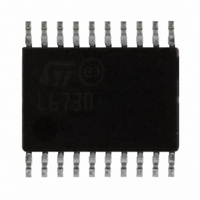
L6730TR STMicroelectronics, L6730TR Datasheet - Page 8

L6730TR
Manufacturer Part Number
L6730TR
Description
IC CTRLR ADJ STEP DOWN 20-TSSOP
Manufacturer
STMicroelectronics
Type
Step-Down (Buck)r
Datasheet
1.L6730TR.pdf
(52 pages)
Specifications of L6730TR
Internal Switch(s)
No
Synchronous Rectifier
Yes
Number Of Outputs
1
Voltage - Output
Adj to 0.6V
Frequency - Switching
100kHz ~ 1MHz
Voltage - Input
1.8 ~ 14 V
Operating Temperature
-40°C ~ 85°C
Mounting Type
Surface Mount
Package / Case
20-TSSOP Exposed Pad, 20-eTSSOP, 20-HTSSOP
Output Voltage
0.6 V
Input Voltage
1.8 V to 14 V
Maximum Operating Temperature
+ 85 C
Minimum Operating Temperature
- 40 C
For Use With
497-5868 - EVAL BOARD 30A 400KHZ L6730497-5501 - EVAL BOARD FOR L6730XX
Lead Free Status / RoHS Status
Lead free / RoHS Compliant
Current - Output
-
Power - Output
-
Lead Free Status / Rohs Status
Lead free / RoHS Compliant
Other names
497-5098-2
Available stocks
Company
Part Number
Manufacturer
Quantity
Price
Part Number:
L6730TR
Manufacturer:
ST
Quantity:
20 000
Pin connections and functions
3
Note:
8/52
Pin connections and functions
Figure 3.
In the L6730B the multifunction pin is: CC/OVP/UVLO.
Table 4.
Pin n.
1
2
3
SINK/OVP/UVLO
PGOOD DELAY
CC/OVP/UVLO
SYNCH
L6730B
Name
L6730
Pins connection (top view)
Pin connection
SINK/OVP/UVLO
PGOOD DELAY
PGOOD DELAY
A capacitor connected between this pin and GND introduces a delay
between the internal PGOOD comparator trigger and the external signal
rising edge. No delay can be introduced on the falling edge of the
PGOOD signal. The delay can be calculated with the following formula:
Two or more devices can be synchronized by connecting the SYNCH pins
together. The device operating with the highest F
device. The Slave devices will operate at 180° phase shift from the
Master. The best way to synchronize devices is to set their F
same value. If it is not used, the SYNCH pin can be left floating.
With this pin it is possible:
To enable-disable the sink mode current capability after SS (L6730);
To enable-disable the constant current OCP after SS (L6730B);
To enable-disable the latch mode for the OVP;
To set the UVLO threshold for the 5 V BUS and 12 V BUS.
The device captures the analog value present at this pin at the start-up
when V
TMASK
TMASK
EAREF
EAREF
SS/INH
SS/INH
SYNCH
SYNCH
COMP
COMP
GND
GND
OSC
OSC
Doc ID 11938 Rev 3
FB
FB
CC
meets the UVLO threshold.
10
10
1
1
2
2
3
3
4
4
5
5
6
6
7
7
8
8
9
9
HTSSOP20
HTSSOP20
PGDelay
= 5 .
20
20
19
19
18
18
17
17
16
16
15
15
14
14
13
13
12
12
11
11
Description
0
⋅
C
( )
pF
VCC
VCC
PGOOD
PGOOD
VCCDR
VCCDR
PGND
PGND
HGATE
HGATE
PHASE
PHASE
LGATE
LGATE
BOOT
BOOT
OCL
OCL
OCH
OCH
[μs]
SW
will be the Master
L6730 - L6730B
SW
at the


