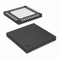
ZL2106ALCN Intersil, ZL2106ALCN Datasheet - Page 12

ZL2106ALCN
Manufacturer Part Number
ZL2106ALCN
Description
IC DCDC CONV STP-DN SYNC 36QFN
Manufacturer
Intersil
Type
Step-Down (Buck)r
Datasheet
1.ZL2106ALCN.pdf
(30 pages)
Specifications of ZL2106ALCN
Internal Switch(s)
Yes
Synchronous Rectifier
Yes
Number Of Outputs
1
Voltage - Output
0.54 ~ 5.5 V
Current - Output
6A
Frequency - Switching
200kHz ~ 1MHz
Voltage - Input
4.5 ~ 14 V
Operating Temperature
-40°C ~ 85°C
Mounting Type
Surface Mount
Package / Case
36-VQFN
Power - Output
3.5W
Lead Free Status / RoHS Status
Lead free / RoHS Compliant
Available stocks
Company
Part Number
Manufacturer
Quantity
Price
Part Number:
ZL2106ALCN
Manufacturer:
ZILKER
Quantity:
20 000
RESISTOR SETTINGS
This method allows a greater range of adjustability when
connecting a finite value resistor (in a specified range) between
the multi-mode pin and SGND.
Standard 1% resistor values are used, and only every fourth E96
resistor value is used so the device can reliably recognize the
value of resistance connected to the pin while eliminating the
error associated with the resistor accuracy. Up to 31 unique
selections are available using a single resistor.
I
ZL2106 functions can be configured via the I
using standard PMBus commands. Additionally, any value that
has been configured using the pin-strap or resistor setting
methods can also be re-configured and/or verified via the
I
The SMBus device address and VOUT_MAX are the only
parameters that must be set by external pins. All other device
parameters can be set via the I
set using the SA pin. VOUT_MAX is determined as 10% greater
than the voltage set by the VSET pin.
Resistor pin-straps are recommended to be used for all available
device parameters to allow a safe initial power-up before
configuration is stored via the I
be accomplished by pin-strapping the undervoltage lockout
threshold (using SS pin) to a value greater than the expected
input voltage, thus preventing the device from enabling prior to
loading a configuration file.
Power Conversion Functional
Description
Internal Bias Regulators and Input Supply
Connections
The ZL2106 employs three internal low dropout (LDO) regulators
to supply bias voltages for internal circuitry, allowing it to operate
from a single input supply. The internal bias regulators are as
follows:
• VR: The VR LDO provides a regulated 7V bias supply for the
• VRA: The VRA LDO provides a regulated 5V bias supply for the
2
2
C/SMBus. See Application Note AN2033 for more details.
FIGURE 13. PIN-STRAP AND RESISTOR SETTING EXAMPLES
C/SMBUS METHOD
high-side MOSFET driver circuit. It is powered from the VDDS
pin and supplies bias current internally. A 4.7µF filter capacitor
is required at the VR pin. The VDDS pin directly supplies the
low-side MOSFET driver circuit.
current sense circuit and other analog circuitry. It is powered
Open
Logic
Logic
high
low
Multi- mode Pin
Pinstrap
Settings
ZL
12
2
2
C/SMBus. For example, this can
C/SMBus. The device address is
R
SET
Multi- mode Pin
2
C/SMBus interface
Resistor
Settings
ZL
ZL2106
• V2P5:The V2P5 LDO provides a regulated 2.5V bias supply for
When the input supply (VDDS) is higher than 7.5V, the VR and
VRA pins should not be connected to any other pins. These pins
should only have a filter capacitor attached. Due to the dropout
voltage associated with the VR and VRA bias regulators, the
VDDS pin must be connected to these pins for designs operating
from a supply below 7.5V. Figure 14 illustrates the required
connections for all cases.
Note: The internal bias regulators, VR and VRA, are not designed
to be outputs for powering other circuitry. Do not attach external
loads to any of these pins. Only the multi-mode pins may be
connected to the V2P5 pin for logic HIGH settings.
High-side Driver Boost Circuit
The gate drive voltage for the high-side MOSFET driver is
generated by a floating bootstrap capacitor, C
When the lower MOSFET (QL) is turned on, the SW node is pulled
to ground and the capacitor is charged from the internal VR bias
regulator through diode D
MOSFET (QH) turns on, the SW node is pulled up to VDDP and the
voltage on the bootstrap capacitor is boosted approximately 6.5V
above VDDP to provide the necessary voltage to power the high-
side driver. An internal Schottky diode is used with C
maximize the high-side drive supply voltage.
Output Voltage Selection
The output voltage may be set to any voltage between 0.6V and
5.0V provided that the input voltage is higher than the desired
output voltage by an amount sufficient to prevent the device
from exceeding its maximum duty cycle specification. Using the
pin-strap method, V
voltages as shown in Table 2.
from the VDDS pin and supplies bias current internally. A
4.7µF filter capacitor is required at the VRA pin.
the main controller circuitry. It is powered from the VRA LDO
and supplies bias current internally. A 10µF filter capacitor is
required at the V2P5 pin.
4.5V ≤ V
VDDS
VRA
TABLE 2. PIN-STRAP OUTPUT VOLTAGE SETTINGS
VR
FIGURE 14. INPUT SUPPLY CONNECTIONS
IN
OPEN
VSET
HIGH
LOW
≤ 5.5V
V
IN
OUT
can be set to one of three standard
5.5V < V
B
. When QL turns off and the upper
VDDS
VRA
VR
IN
≤ 7.5V
V
IN
7.5V < V
VDDS
B
VRA
(see Figure 10).
VR
V
1.2
1.5
3.3
(V)
OUT
IN
B
≤ 14V
V
to help
IN
FN6852.4


