ZL2106ALCN Intersil, ZL2106ALCN Datasheet - Page 17
ZL2106ALCN
Manufacturer Part Number
ZL2106ALCN
Description
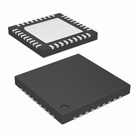
IC DCDC CONV STP-DN SYNC 36QFN
Manufacturer
Intersil
Type
Step-Down (Buck)r
Datasheet
1.ZL2106ALCN.pdf
(30 pages)
Specifications of ZL2106ALCN
Internal Switch(s)
Yes
Synchronous Rectifier
Yes
Number Of Outputs
1
Voltage - Output
0.54 ~ 5.5 V
Current - Output
6A
Frequency - Switching
200kHz ~ 1MHz
Voltage - Input
4.5 ~ 14 V
Operating Temperature
-40°C ~ 85°C
Mounting Type
Surface Mount
Package / Case
36-VQFN
Power - Output
3.5W
Lead Free Status / RoHS Status
Lead free / RoHS Compliant
Available stocks
Company
Part Number
Manufacturer
Quantity
Price

Part Number:
ZL2106ALCN
Manufacturer:
ZILKER
Quantity:
20 000


between output ripple and optimal load transient performance. A
good starting point is to select the output inductor ripple equal to
the expected load transient step magnitude (I
Now the output inductance can be calculated using Equation 3,
where V
The average inductor current is equal to the maximum output
current. The peak inductor current (I
Equation 4 where I
Select an inductor rated for the average DC current with a peak
current rating above the peak current computed in Equation 4.
In overcurrent or short-circuit conditions, the inductor may have
currents greater than 2X the normal maximum rated output
current. It is desirable to use an inductor that still provides some
inductance to protect the load and the internal MOSFETs from
damaging currents in this situation.
Once an inductor is selected, the DCR and core losses in the
inductor are calculated. Use the DCR specified in the inductor
manufacturer’s data sheet.
I
where I
core loss of the selected inductor. Since this calculation is
specific to each inductor and manufacturer, refer to the chosen
inductor data sheet. Add the core loss and the DCR loss and
compare the total loss to the maximum power dissipation
recommendation in the inductor data sheet.
OUTPUT CAPACITOR SELECTION
Several trade-offs must also be considered when selecting an
output capacitor. Low ESR values are needed to have a small
output deviation during transient load steps (V
output voltage ripple (V
such as semi-stable (X5R and X7R) dielectric ceramic capacitors,
also have relatively low capacitance values. Many designs can
use a combination of high capacitance devices and low ESR
devices in parallel.
For high ripple currents, a low capacitance value can cause a
significant amount of output voltage ripple. Likewise, in high
transient load steps, a relatively large amount of capacitance is
needed to minimize the output voltage deviation while the
inductor current ramps up or down to the new steady state
output current value.
I
L
I
P
I
Lrms
opp
Lpk
Lrms
LDCR
OUT
is given by Equation 6:
=
=
=
=
OUT
INM
=
I
I
V
ostep
OUT
DCR
is the maximum output current. Next, calculate the
OUT
is the maximum input voltage:
I
OUT
+
fsw
×
×
2
I
⎛
⎜ ⎜
⎝
OUT
opp
+
2
I
1
×
Lrms
−
( )
I
is the maximum output current:
I
orip
opp
opp
12
V
V
2
OUT
INM
). However, capacitors with low ESR,
2
17
⎞
⎟ ⎟
⎠
Lpk
) is calculated using
ostep
osag
):
) and low
(EQ. 2)
(EQ. 3)
(EQ. 5)
(EQ. 6)
(EQ. 4)
ZL2106
As a starting point, apportion one-half of the output ripple
voltage to the capacitor ESR and the other half to capacitance, as
shown in Equations 7 and 8:
Use these values to make an initial capacitor selection, using a
single capacitor or several capacitors in parallel.
After a capacitor has been selected, the resulting output voltage
ripple can be calculated using Equation 9:
Because each part of this equation was made to be less than or
equal to half of the allowed output ripple voltage, the V
be less than the desired maximum output ripple.
INPUT CAPACITOR
It is highly recommended that dedicated input capacitors be
used in any point-of-load design, even when the supply is
powered from a heavily filtered 5V or 12V “bulk” supply from an
off-line power supply. This is because of the high RMS ripple
current that is drawn by the buck converter topology. This ripple
(I
Without capacitive filtering near the power supply circuit, this
current would flow through the supply bus and return planes,
coupling noise into other system circuitry. The input capacitors
should be rated at 1.2X the ripple current calculated in Equation
10 to avoid overheating of the capacitors due to the high ripple
current, which can cause premature failure. Ceramic capacitors
with X7R or X5R dielectric with low ESR and 1.1X the maximum
expected input voltage are recommended.
BOOTSTRAP CAPACITOR SELECTION
The high-side driver boost circuit utilizes an internal Schottky
diode (D
sufficient gate drive for the high-side MOSFET driver. C
be a 47nF ceramic type rated for at least 10V.
C
This capacitor is used to both stabilize and provide noise filtering
for the 2.5V internal power supply. It should be between 4.7µF
and 10µF, should use a semi-stable X5R or X7R dielectric
ceramic with a low ESR (less than 10mΩ) and should have a
rating of 4V or more.
C
This capacitor is used to both stabilize and provide noise filtering
for the 7V reference supply. It should be between 4.7µF and
10µF, should use a semi-stable X5R or X7R dielectric ceramic
capacitor with a low ESR (less than 10mΩ) and should have a
rating of 10V or more. Because the current for the bootstrap
supply is drawn from this capacitor, C
V
C
ESR
I
CINrms
V2P5
VR
CINrms
orip
OUT
SELECTION
=
=
) can be determined from Equation 10:
SELECTION
=
B
=
I
2
) and an external bootstrap capacitor (C
8
opp
V
×
I
×
OUT
orip
I
×
f
opp
sw
ESR
I
×
opp
×
V
D
+
orip
2
×
8
×
1 ( D
f
−
sw
I
opp
×
)
C
VR
OUT
should be sized at least
B
) to supply
orip
B
should
(EQ. 10)
FN6852.4
should
(EQ. 7)
(EQ. 8)
(EQ. 9)
Related parts for ZL2106ALCN
Image
Part Number
Description
Manufacturer
Datasheet
Request
R

Part Number:
Description:
6a Digital-dc Synchronous Step-down Dc-dc Converter
Manufacturer:
Intersil Corporation
Datasheet:
Part Number:
Description:
Intersil Corporation [CMOS Serial Controller Interface]
Manufacturer:
Intersil Corporation
Datasheet:
Part Number:
Description:
Manufacturer:
Intersil Corporation
Datasheet:
Part Number:
Description:
357-036-542-201 CARDEDGE 36POS DL .156 BLK LOPRO
Manufacturer:
Intersil Corporation
Datasheet:
Part Number:
Description:
1024-Word x 4-Bit LSI Static RAM
Manufacturer:
Intersil Corporation
Datasheet:
Part Number:
Description:
General Purpose NPN Transistor Arrays FN341.4
Manufacturer:
Intersil Corporation
Datasheet:
Part Number:
Description:
CMOS 16-Bit Microprocessor
Manufacturer:
Intersil Corporation
Datasheet:
Part Number:
Description:
Manufacturer:
Intersil Corporation
Datasheet:
Part Number:
Description:
Manufacturer:
Intersil Corporation
Datasheet:
Part Number:
Description:
Manufacturer:
Intersil Corporation
Datasheet:
Part Number:
Description:
Manufacturer:
Intersil Corporation
Datasheet:
Part Number:
Description:
CMOS 6-Bit Latch and Decoder Memory Interfaces
Manufacturer:
Intersil Corporation
Datasheet:
Part Number:
Description:
CA3046General Purpose NPN Transistor Arrays
Manufacturer:
Intersil Corporation
Datasheet:
Part Number:
Description:
Manufacturer:
Intersil Corporation
Datasheet:
Part Number:
Description:
TR909 DLC/FLC SLIC with Low Power Standby
Manufacturer:
Intersil Corporation
Datasheet: