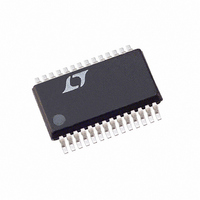
LTC3890EGN-1#PBF Linear Technology, LTC3890EGN-1#PBF Datasheet - Page 12

LTC3890EGN-1#PBF
Manufacturer Part Number
LTC3890EGN-1#PBF
Description
IC BUCK SYNC ADJ 25A DUAL 28SSOP
Manufacturer
Linear Technology
Type
Step-Down (Buck)r
Specifications of LTC3890EGN-1#PBF
Internal Switch(s)
No
Synchronous Rectifier
Yes
Number Of Outputs
2
Voltage - Output
0.8 ~ 24 V
Current - Output
25A
Frequency - Switching
50kHz ~ 900kHz
Voltage - Input
4 ~ 60 V
Operating Temperature
-40°C ~ 125°C
Mounting Type
Surface Mount
Package / Case
28-SSOP
Primary Input Voltage
12V
No. Of Outputs
2
Output Voltage
24V
Output Current
25A
No. Of Pins
32
Operating Temperature Range
-40°C To +125°C
Msl
MSL 1 - Unlimited
Supply Voltage Min
4V
Rohs Compliant
Yes
Lead Free Status / RoHS Status
Lead free / RoHS Compliant
Power - Output
-
OPERATION
LTC3890
Light Load Current Operation (Burst Mode Operation,
Pulse-Skipping or Forced Continuous Mode)
(PLLIN/MODE Pin)
The LTC3890 can be enabled to enter high efficiency Burst
Mode operation, constant frequency pulse-skipping mode,
or forced continuous conduction mode at low load currents.
To select Burst Mode operation, tie the PLLIN/ MODE pin
to a DC voltage below 0.8V (e.g., SGND). To select forced
continuous operation, tie the PLLIN/MODE pin to INTV
To select pulse-skipping mode, tie the PLLIN/MODE pin to
a DC voltage greater than 1.2V and less than INTV
When a controller is enabled for Burst Mode operation, the
minimum peak current in the inductor is set to approxi-
mately 25% of the maximum sense voltage even though
the voltage on the ITH pin indicates a lower value. If the
average inductor current is higher than the load current,
the error amplifier, EA, will decrease the voltage on the
ITH pin. When the ITH voltage drops below 0.425V, the
internal sleep signal goes high (enabling sleep mode)
and both external MOSFETs are turned off. The ITH pin is
then disconnected from the output of the EA and parked
at 0.450V.
In sleep mode, much of the internal circuitry is turned off,
reducing the quiescent current that the LTC3890 draws.
If one channel is shut down and the other channel is in
sleep mode, the LTC3890 draws only 50μA of quiescent
current. If both channels are in sleep mode, the LTC3890
draws only 60μA of quiescent current. In sleep mode,
the load current is supplied by the output capacitor. As
the output voltage decreases, the EA’s output begins to
rise. When the output voltage drops enough, the ITH pin
is reconnected to the output of the EA, the sleep signal
goes low, and the controller resumes normal operation
by turning on the top external MOSFET on the next cycle
of the internal oscillator.
When a controller is enabled for Burst Mode operation, the
inductor current is not allowed to reverse. The reverse cur-
rent comparator, IR, turns off the bottom external MOSFET
just before the inductor current reaches zero, preventing
it from reversing and going negative. Thus, the controller
operates in discontinuous operation.
12
(Refer to the Functional Diagram)
CC
– 1.3V.
CC
.
In forced continuous operation or clocked by an external
clock source to use the phase-locked loop (see Frequency
Selection and Phase-Locked Loop section), the induc-
tor current is allowed to reverse at light loads or under
large transient conditions. The peak inductor current is
determined by the voltage on the ITH pin, just as in normal
operation. In this mode, the efficiency at light loads is lower
than in Burst Mode operation. However, continuous opera-
tion has the advantage of lower output voltage ripple and
less interference to audio circuitry. In forced continuous
mode, the output ripple is independent of load current.
When the PLLIN/MODE pin is connected for pulse-skipping
mode, the LTC3890 operates in PWM pulse-skipping
mode at light loads. In this mode, constant frequency
operation is maintained down to approximately 1% of
designed maximum output current. At very light loads, the
current comparator, ICMP , may remain tripped for several
cycles and force the external top MOSFET to stay off for
the same number of cycles (i.e., skipping pulses). The
inductor current is not allowed to reverse (discontinuous
operation). This mode, like forced continuous operation,
exhibits low output ripple as well as low audio noise and
reduced RF interference as compared to Burst Mode
operation. It provides higher low current efficiency than
forced continuous mode, but not nearly as high as Burst
Mode operation.
Frequency Selection and Phase-Locked Loop
(FREQ and PLLIN/MODE Pins)
The selection of switching frequency is a trade-off between
efficiency and component size. Low frequency opera-
tion increases efficiency by reducing MOSFET switching
losses, but requires larger inductance and/or capacitance
to maintain low output ripple voltage.
The switching frequency of the LTC3890’s controllers can
be selected using the FREQ pin.
If the PLLIN/MODE pin is not being driven by an external
clock source, the FREQ pin can be tied to SGND, tied to
INTV
FREQ to SGND selects 350kHz while tying FREQ to INTV
selects 535kHz. Placing a resistor between FREQ and SGND
allows the frequency to be programmed between 50kHz
and 900kHz, as shown in Figure 10.
CC
or programmed through an external resistor. Tying
3890fa
CC


