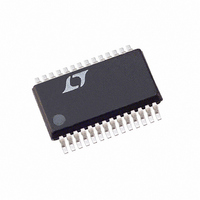
LTC3890EGN-1#PBF Linear Technology, LTC3890EGN-1#PBF Datasheet - Page 23

LTC3890EGN-1#PBF
Manufacturer Part Number
LTC3890EGN-1#PBF
Description
IC BUCK SYNC ADJ 25A DUAL 28SSOP
Manufacturer
Linear Technology
Type
Step-Down (Buck)r
Specifications of LTC3890EGN-1#PBF
Internal Switch(s)
No
Synchronous Rectifier
Yes
Number Of Outputs
2
Voltage - Output
0.8 ~ 24 V
Current - Output
25A
Frequency - Switching
50kHz ~ 900kHz
Voltage - Input
4 ~ 60 V
Operating Temperature
-40°C ~ 125°C
Mounting Type
Surface Mount
Package / Case
28-SSOP
Primary Input Voltage
12V
No. Of Outputs
2
Output Voltage
24V
Output Current
25A
No. Of Pins
32
Operating Temperature Range
-40°C To +125°C
Msl
MSL 1 - Unlimited
Supply Voltage Min
4V
Rohs Compliant
Yes
Lead Free Status / RoHS Status
Lead free / RoHS Compliant
Power - Output
-
Fault Conditions: Current Limit and Current Foldback
The LTC3890 includes current foldback to help limit
load current when the output is shorted to ground. If
the output voltage falls below 70% of its nominal output
level, then the maximum sense voltage is progressively
lowered from 100% to 45% of its maximum selected
value. Under short-circuit conditions with very low duty
cycles, the LTC3890 will begin cycle skipping in order to
limit the short-circuit current. In this situation the bottom
MOSFET will be dissipating most of the power but less
than in normal operation. The short-circuit ripple current
is determined by the minimum on-time, t
LTC3890 (≈95ns), the input voltage and inductor value:
The resulting average short-circuit current is:
Fault Conditions: Overvoltage Protection (Crowbar)
The overvoltage crowbar is designed to blow a system
input fuse when the output voltage of the regulator rises
much higher than nominal levels. The crowbar causes huge
currents to flow, that blow the fuse to protect against a
shorted top MOSFET if the short occurs while the control-
ler is operating.
A comparator monitors the output for overvoltage condi-
tions. The comparator detects faults greater than 10%
above the nominal output voltage. When this condition
is sensed, the top MOSFET is turned off and the bottom
MOSFET is turned on until the overvoltage condition is
cleared. The bottom MOSFET remains on continuously for
as long as the overvoltage condition persists; if V
to a safe level, normal operation automatically resumes.
A shorted top MOSFET will result in a high current condition
which will open the system fuse. The switching regulator
will regulate properly with a leaky top MOSFET by altering
the duty cycle to accommodate the leakage.
APPLICATIONS INFORMATION
I
ΔI
SC
L(SC)
= 45% • I
= t
ON(MIN)
LIM(MAX)
⎛
⎜
⎝
V
L
IN
–
⎞
⎟
⎠
2
1
ΔI
L(SC)
ON(MIN)
OUT
, of the
returns
Phase-Locked Loop and Frequency Synchronization
The LTC3890 has an internal phase-locked loop (PLL)
comprised of a phase frequency detector, a lowpass filter,
and a voltage-controlled oscillator (VCO). This allows the
turn-on of the top MOSFET of controller 1 to be locked to
the rising edge of an external clock signal applied to the
PLLIN/MODE pin. The turn-on of controller 2’s top MOSFET
is thus 180 degrees out of phase with the external clock.
The phase detector is an edge sensitive digital type that
provides zero degrees phase shift between the external
and internal oscillators. This type of phase detector does
not exhibit false lock to harmonics of the external clock.
If the external clock frequency is greater than the internal
oscillator’s frequency, f
ously from the phase detector output, pulling up the VCO
input. When the external clock frequency is less than f
current is sunk continuously, pulling down the VCO input.
If the external and internal frequencies are the same but
exhibit a phase difference, the current sources turn on for
an amount of time corresponding to the phase difference.
The voltage at the VCO input is adjusted until the phase
and frequency of the internal and external oscillators are
identical. At the stable operating point, the phase detector
output is high impedance and the internal filter capacitor,
C
LP
, holds the voltage at the VCO input.
Figure 10. Relationship Between Oscillator Frequency
and Resistor Value at the FREQ Pin
1000
900
800
700
400
300
200
100
600
500
0
15
25
35 45 55
FREQ PIN RESISTOR (kΩ)
OSC
, then current is sourced continu-
65 75 85 95 105 115 125
LTC3890
3890 F10
23
OSC
3890fa
,


