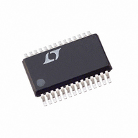
LTC3890EGN-1#PBF Linear Technology, LTC3890EGN-1#PBF Datasheet - Page 21

LTC3890EGN-1#PBF
Manufacturer Part Number
LTC3890EGN-1#PBF
Description
IC BUCK SYNC ADJ 25A DUAL 28SSOP
Manufacturer
Linear Technology
Type
Step-Down (Buck)r
Specifications of LTC3890EGN-1#PBF
Internal Switch(s)
No
Synchronous Rectifier
Yes
Number Of Outputs
2
Voltage - Output
0.8 ~ 24 V
Current - Output
25A
Frequency - Switching
50kHz ~ 900kHz
Voltage - Input
4 ~ 60 V
Operating Temperature
-40°C ~ 125°C
Mounting Type
Surface Mount
Package / Case
28-SSOP
Primary Input Voltage
12V
No. Of Outputs
2
Output Voltage
24V
Output Current
25A
No. Of Pins
32
Operating Temperature Range
-40°C To +125°C
Msl
MSL 1 - Unlimited
Supply Voltage Min
4V
Rohs Compliant
Yes
Lead Free Status / RoHS Status
Lead free / RoHS Compliant
Power - Output
-
INTV
The LTC3890 features two separate internal P-channel low
dropout linear regulators (LDO) that supply power at the
INTV
pin depending on the connection of the EXTV
INTV
internal circuitry. The V
INTV
50mA and must be bypassed to ground with a minimum
of 4.7μF ceramic capacitor. No matter what type of bulk
capacitor is used, an additional 1μF ceramic capacitor
placed directly adjacent to the INTV
highly recommended. Good bypassing is needed to supply
the high transient currents required by the MOSFET gate
drivers and to prevent interaction between the channels.
High input voltage applications in which large MOSFETs
are being driven at high frequencies may cause the maxi-
mum junction temperature rating for the LTC3890 to be
exceeded. The INTV
the gate charge current, may be supplied by either the
V
EXTV
dissipation for the IC in this case is highest and is equal
to V
operating frequency as discussed in the Efficiency Consid-
erations section. The junction temperature can be estimated
by using the equations given in Note 3 of the Electrical
Characteristics. For example, the LTC3890 INTV
is limited to less than 32mA from a 40V supply when not
using the EXTV
APPLICATIONS INFORMATION
IN
T
IN
J
LDO or the EXTV
CC
CC
CC
CC
CC
= 70°C + (32mA)(40V)(43°C/W) = 125°C
• I
powers the gate drivers and much of the LTC3890’s
to 5.1V. Each of these can supply a peak current of
Regulators
pin from either the V
pin is less than 4.7V, the V
INTVCC
. The gate charge current is dependent on
CC
supply at a 70°C ambient temperature:
CC
IN
CC
current, which is dominated by
LDO and the EXTV
LDO. When the voltage on the
IN
supply pin or the EXTV
IN
LDO is enabled. Power
CC
and PGND pins is
CC
LDO regulate
CC
CC
current
pin.
CC
To prevent the maximum junction temperature from be-
ing exceeded, the input supply current must be checked
while operating in forced continuous mode (PLLIN/MODE
= INTV
When the voltage applied to EXTV
V
EXTV
EXTV
to regulate the INTV
is less than 5.1V, the LDO is in dropout and the INTV
voltage is approximately equal to EXTV
is greater than 5.1V, up to an absolute maximum of 14V,
INTV
Using the EXTV
control power to be derived from one of the LTC3890’s
switching regulator outputs (4.7V ≤ V
normal operation and from the V
is out of regulation (e.g., start-up, short-circuit). If more
current is required through the EXTV
fied, an external Schottky diode can be added between the
EXTV
than 6V to the EXTV
Significant efficiency and thermal gains can be realized
by powering INTV
rent resulting from the driver and control currents will be
scaled by a factor of (Duty Cycle)/(Switcher Efficiency).
For 5V to 14V regulator outputs, this means connecting
the EXTV
an 8.5V supply reduces the junction temperature in the
previous example from 125°C to:
However, for 3.3V and other low voltage outputs, additional
circuitry is required to derive INTV
IN
T
LDO is turned off and the EXTV
J
CC
CC
CC
CC
= 70°C + (32mA)(8.5V)(43°C/W) = 82°C
CC
is regulated to 5.1V.
LDO remains on as long as the voltage applied to
and INTV
remains above 4.5V. The EXTV
) at maximum V
CC
pin directly to V
CC
CC
CC
CC
LDO allows the MOSFET driver and
pins. In this case, do not apply more
CC
pin and make sure that EXTV
from the output, since the V
voltage to 5.1V, so while EXTV
IN
.
OUT
. Tying the EXTV
CC
IN
CC
CC
power from the output.
LDO when the output
CC
rises above 4.7V, the
LDO is enabled. The
OUT
LDO than is speci-
CC
LTC3890
CC
. When EXTV
LDO attempts
≤ 14V) during
CC
CC
21
IN
pin to
≤ V
3890fa
cur-
IN
CC
CC
CC
.


