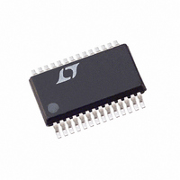
LTC3890EGN-1#PBF Linear Technology, LTC3890EGN-1#PBF Datasheet - Page 24

LTC3890EGN-1#PBF
Manufacturer Part Number
LTC3890EGN-1#PBF
Description
IC BUCK SYNC ADJ 25A DUAL 28SSOP
Manufacturer
Linear Technology
Type
Step-Down (Buck)r
Specifications of LTC3890EGN-1#PBF
Internal Switch(s)
No
Synchronous Rectifier
Yes
Number Of Outputs
2
Voltage - Output
0.8 ~ 24 V
Current - Output
25A
Frequency - Switching
50kHz ~ 900kHz
Voltage - Input
4 ~ 60 V
Operating Temperature
-40°C ~ 125°C
Mounting Type
Surface Mount
Package / Case
28-SSOP
Primary Input Voltage
12V
No. Of Outputs
2
Output Voltage
24V
Output Current
25A
No. Of Pins
32
Operating Temperature Range
-40°C To +125°C
Msl
MSL 1 - Unlimited
Supply Voltage Min
4V
Rohs Compliant
Yes
Lead Free Status / RoHS Status
Lead free / RoHS Compliant
Power - Output
-
LTC3890
Note that the LTC3890 can only be synchronized to an
external clock whose frequency is within range of the
LTC3890’s internal VCO, which is nominally 55kHz to
1MHz. This is guaranteed to be between 75kHz and 850kHz.
Typically, the external clock (on the PLLIN/MODE pin) input
high threshold is 1.6V, while the input low threshold is 1.1V.
Rapid phase locking can be achieved by using the FREQ pin
to set a free-running frequency near the desired synchro-
nization frequency. The VCO’s input voltage is prebiased
at a frequency corresponding to the frequency set by the
FREQ pin. Once prebiased, the PLL only needs to adjust
the frequency slightly to achieve phase lock and synchro-
nization. Although it is not required that the free-running
frequency be near external clock frequency, doing so will
prevent the operating frequency from passing through a
large range of frequencies as the PLL locks.
Table 2 summarizes the different states in which the FREQ
pin can be used.
Table 2
24
APPLICATIONS INFORMATION
Any of the Above
FREQ PIN
Resistor
INTV
0V
CC
PLLIN/MODE PIN
External Clock
DC Voltage
DC Voltage
DC Voltage
50kHz to 900kHz
Phase Locked to
External Clock
FREQUENCY
350kHz
535kHz
Minimum On-Time Considerations
Minimum on-time, t
that the LTC3890 is capable of turning on the top MOSFET.
It is determined by internal timing delays and the gate
charge required to turn on the top MOSFET. Low duty
cycle applications may approach this minimum on-time
limit and care should be taken to ensure that:
If the duty cycle falls below what can be accommodated
by the minimum on-time, the controller will begin to skip
cycles. The output voltage will continue to be regulated,
but the ripple voltage and current will increase.
The minimum on-time for the LTC3890 is approximately
95ns. However, as the peak sense voltage decreases
the minimum on-time gradually increases up to about
130ns. This is of particular concern in forced continuous
applications with low ripple current at light loads. If the
duty cycle drops below the minimum on-time limit in this
situation, a significant amount of cycle skipping can occur
with correspondingly larger current and voltage ripple.
t
ON(MIN)
<
V
V
IN
OUT
( )
f
ON(MIN)
, is the smallest time duration
3890fa


