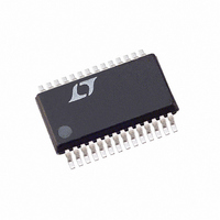
LTC3890EGN-1#PBF Linear Technology, LTC3890EGN-1#PBF Datasheet - Page 30

LTC3890EGN-1#PBF
Manufacturer Part Number
LTC3890EGN-1#PBF
Description
IC BUCK SYNC ADJ 25A DUAL 28SSOP
Manufacturer
Linear Technology
Type
Step-Down (Buck)r
Specifications of LTC3890EGN-1#PBF
Internal Switch(s)
No
Synchronous Rectifier
Yes
Number Of Outputs
2
Voltage - Output
0.8 ~ 24 V
Current - Output
25A
Frequency - Switching
50kHz ~ 900kHz
Voltage - Input
4 ~ 60 V
Operating Temperature
-40°C ~ 125°C
Mounting Type
Surface Mount
Package / Case
28-SSOP
Primary Input Voltage
12V
No. Of Outputs
2
Output Voltage
24V
Output Current
25A
No. Of Pins
32
Operating Temperature Range
-40°C To +125°C
Msl
MSL 1 - Unlimited
Supply Voltage Min
4V
Rohs Compliant
Yes
Lead Free Status / RoHS Status
Lead free / RoHS Compliant
Power - Output
-
PC Board Layout Checklist
When laying out the printed circuit board, the following
checklist should be used to ensure proper operation of
the IC. These items are also illustrated graphically in the
layout diagram of Figure 11. Figure 12 illustrates the current
waveforms present in the various branches of the 2-phase
synchronous regulators operating in the continuous mode.
Check the following in your layout:
1. Are the top N-channel MOSFETs MTOP1 and MTOP2
2. Are the signal and power grounds kept separate? The
3. Do the LTC3890 V
LTC3890
APPLICATIONS INFORMATION
30
located within 1cm of each other with a common drain
connection at C
decoupling for the two channels as it can cause a large
resonant loop.
combined IC signal ground pin and the ground return
of C
minals. The path formed by the top N-channel MOSFET,
Schottky diode and the C
leads and PC trace lengths. The output capacitor (–)
terminals should be connected as close as possible
to the (–) terminals of the input capacitor by placing
the capacitors next to each other and away from the
Schottky loop described above.
the (+) terminals of C
connected between the (+) terminal of C
ground. The feedback resistor connections should not
be along the high current input feeds from the input
capacitor(s).
INTVCC
must return to the combined C
IN
FB
? Do not attempt to split the input
pins’ resistive dividers connect to
OUT
? The resistive divider must be
IN
capacitor should have short
OUT
OUT
and signal
(–) ter-
4. Are the SENSE
5. Is the INTV
6. Keep the switching nodes (SW1, SW2), top gate nodes
7. Use a modified star ground technique: a low impedance,
minimum PC trace spacing? The filter capacitor between
SENSE
to the IC. Ensure accurate current sensing with Kelvin
connections at the SENSE resistor.
to the IC, between the INTV
pins? This capacitor carries the MOSFET drivers’ cur-
rent peaks. An additional 1μF ceramic capacitor placed
immediately next to the INTV
improve noise performance substantially.
(TG1, TG2), and boost nodes (BOOST1, BOOST2) away
from sensitive small-signal nodes, especially from
the opposites channel’s voltage and current sensing
feedback pins. All of these nodes have very large and
fast moving signals and therefore should be kept on
the output side of the LTC3890 and occupy minimum
PC trace area.
large copper area central grounding point on the same
side of the PC board as the input and output capacitors
with tie-ins for the bottom of the INTV
capacitor, the bottom of the voltage feedback resistive
divider and the SGND pin of the IC.
+
and SENSE
CC
–
decoupling capacitor connected close
and SENSE
–
should be as close as possible
+
CC
leads routed together with
CC
and PGND pins can help
and the power ground
CC
decoupling
3890fa


