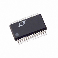
LTC3890EGN-1#PBF Linear Technology, LTC3890EGN-1#PBF Datasheet - Page 13

LTC3890EGN-1#PBF
Manufacturer Part Number
LTC3890EGN-1#PBF
Description
IC BUCK SYNC ADJ 25A DUAL 28SSOP
Manufacturer
Linear Technology
Type
Step-Down (Buck)r
Specifications of LTC3890EGN-1#PBF
Internal Switch(s)
No
Synchronous Rectifier
Yes
Number Of Outputs
2
Voltage - Output
0.8 ~ 24 V
Current - Output
25A
Frequency - Switching
50kHz ~ 900kHz
Voltage - Input
4 ~ 60 V
Operating Temperature
-40°C ~ 125°C
Mounting Type
Surface Mount
Package / Case
28-SSOP
Primary Input Voltage
12V
No. Of Outputs
2
Output Voltage
24V
Output Current
25A
No. Of Pins
32
Operating Temperature Range
-40°C To +125°C
Msl
MSL 1 - Unlimited
Supply Voltage Min
4V
Rohs Compliant
Yes
Lead Free Status / RoHS Status
Lead free / RoHS Compliant
Power - Output
-
OPERATION
A phase-locked loop (PLL) is available on the LTC3890
to synchronize the internal oscillator to an external clock
source that is connected to the PLLIN/MODE pin. The
LTC3890’s phase detector adjusts the voltage (through
an internal lowpass filter) of the VCO input to align the
turn-on of controller 1’s external top MOSFET to the ris-
ing edge of the synchronizing signal. Thus, the turn-on
of controller 2’s external top MOSFET is 180 degrees out
of phase to the rising edge of the external clock source.
The VCO input voltage is prebiased to the operating fre-
quency set by the FREQ pin before the external clock is
applied. If prebiased near the external clock frequency,
the PLL loop only needs to make slight changes to the
VCO input in order to synchronize the rising edge of the
external clock’s to the rising edge of TG1. The ability to
prebias the loop filter allows the PLL to lock-in rapidly
without deviating far from the desired frequency.
The typical capture range of the phase-locked loop is from
approximately 55kHz to 1MHz, with a guarantee to be
between 75kHz and 850kHz. In other words, the LTC3890’s
PLL is guaranteed to lock to an external clock source whose
frequency is between 75kHz and 850kHz.
The typical input clock thresholds on the PLLIN/MODE
pin are 1.6V (rising) and 1.2V (falling).
PolyPhase Applications (CLKOUT and PHASMD Pins)
The LTC3890 features two pins (CLKOUT and PHASMD)
that allow other controller ICs to be daisy-chained with
the LTC3890 in PolyPhase applications. The clock output
signal on the CLKOUT pin can be used to synchronize
additional power stages in a multiphase power supply
solution feeding a single, high current output or multiple
separate outputs. The PHASMD pin is used to adjust the
phase of the CLKOUT signal as well as the relative phases
between the two internal controllers, as summarized in
Table 1. The phases are calculated relative to the zero
degrees phase being defined as the rising edge of the top
gate driver output of controller 1 (TG1).
Table 1
V
Floating
INTV
PHASMD
GND
CC
CONTROLLER 2 PHASE
(Refer to the Functional Diagram)
180°
180°
240°
CLKOUT PHASE
120°
60°
90°
Output Overvoltage Protection
An overvoltage comparator guards against transient over-
shoots as well as other more serious conditions that may
overvoltage the output. When the V
than 10% above its regulation point of 0.800V, the top
MOSFET is turned off and the bottom MOSFET is turned
on until the overvoltage condition is cleared.
Power Good (PGOOD1 and PGOOD2) Pins
Each PGOOD pin is connected to an open drain of an
internal N-channel MOSFET. The MOSFET turns on and
pulls the PGOOD pin low when the corresponding V
voltage is not within ±10% of the 0.8V reference voltage.
The PGOOD pin is also pulled low when the corresponding
RUN pin is low (shut down). When the V
is within the ±10% requirement, the MOSFET is turned
off and the pin is allowed to be pulled up by an external
resistor to a source no greater than 6V.
Foldback Current
When the output voltage falls to less than 70% of its
nominal level, foldback current limiting is activated, pro-
gressively lowering the peak current limit in proportion to
the severity of the overcurrent or short-circuit condition.
Foldback current limiting is disabled during the soft-start
interval (as long as the V
TRACK/SS voltage).
Theory and Benefits of 2-Phase Operation
Why the need for 2-phase operation? Up until the 2-phase
family, constant-frequency dual switching regulators
operated both channels in phase (i.e., single phase
operation). This means that both switches turned on at
the same time, causing current pulses of up to twice the
amplitude of those for one regulator to be drawn from the
input capacitor and battery. These large amplitude current
pulses increased the total RMS current flowing from the
input capacitor, requiring the use of more expensive input
capacitors and increasing both EMI and losses in the input
capacitor and battery.
FB
voltage is keeping up with the
FB
pin rises by more
LTC3890
FB
pin voltage
13
FB
3890fa
pin


