LM26001QMXAX/NOPB National Semiconductor, LM26001QMXAX/NOPB Datasheet - Page 10
LM26001QMXAX/NOPB
Manufacturer Part Number
LM26001QMXAX/NOPB
Description
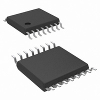
IC REG SW 1.5A W/SLEEP 16-TSSOP
Manufacturer
National Semiconductor
Series
PowerWise®r
Type
Step-Down (Buck)r
Datasheet
1.LM26001QMXANOPB.pdf
(18 pages)
Specifications of LM26001QMXAX/NOPB
Internal Switch(s)
Yes
Synchronous Rectifier
No
Number Of Outputs
1
Voltage - Output
1.25 ~ 35 V
Current - Output
1.5A
Frequency - Switching
150kHz ~ 500kHz
Voltage - Input
4 ~ 38 V
Operating Temperature
-40°C ~ 125°C
Mounting Type
Surface Mount
Package / Case
16-TSSOP Exposed Pad, 16-eTSSOP, 16-HTSSOP
Power - Output
2.6W
Lead Free Status / RoHS Status
Lead free / RoHS Compliant
Other names
LM26001QMXAX
Available stocks
Company
Part Number
Manufacturer
Quantity
Price
Company:

Part Number:
LM26001QMXAX/NOPB
Manufacturer:
MOLEX
Quantity:
10 000


www.national.com
Where I
I
And Io is the sum of Iload, Ibias, and current through the
feedback resistors.
Because this calculation applies only to sleep mode, use the
I
is connected to ground, use the same equation with Ibias
equal to zero and I
FPWM
Pulling the FPWM pin high disables sleep mode and forces
the LM26001 to always operate in PWM mode. Light load ef-
ficiency is reduced in PWM mode, but switching frequency
remains stable. The FPWM pin can be connected to the VDD
pin to pull it high. In FPWM mode, under light load conditions,
the regulator operates in discontinuous conduction mode
(DCM) . In discontinuous conduction mode, current through
the inductor starts at zero and ramps up to its peak, then
ramps down to zero again. Until the next cycle, the inductor
current remains at zero. At nominal load currents, in FPWM
mode, the device operates in continuous conduction mode,
where positive current always flows in the inductor. Typical
discontinuous operation waveforms are shown below.
At very light load, in FPWM mode, the LM26001 may enter
sleep mode. This is to prevent an over-voltage condition from
occurring. However, the FPWM sleep threshold is much lower
than in normal operation.
ENABLE
The LM26001 provides a shutdown function via the EN pin to
disable the device when the output voltage does not need to
be maintained. EN is an analog level input with typically
120 mV of hysteresis. The device is active when the EN pin
is above 1.2V (typical) and in shutdown mode when EN is
below this threshold. When EN goes high, the internal VDD
regulator turns on and charges the VDD capacitor. When
VDD reaches 3.9V (typical), the soft-start pin begins to source
current. In shutdown mode, the VDD regulator shuts down
and total quiescent current is reduced to 10 µA (typical). Be-
cause the EN pin sources 4.5 µA (typical) of pull-up current,
this pin can be left open for always-on operation. When open,
EN will be pulled up to VIN.
If EN is connected to VIN, it must be connected through a 10
kΩ resistor to limit noise spikes. EN can also be driven exter-
QG
q_Sleep_VB
= (4.6 x 10
FIGURE 4. Discontinuous Mode Waveforms
QG
and I
is the gate drive current, calculated as:
Iin = Iq + (I
-9
BIAS_SLEEP
) x f
75mA Load, Vin = 12V
q_Sleep_VDD
SW
QG
values from the EC table. If VBIAS
x Dwake) + (Io x D)
.
20179423
10
nally with a maximum voltage of 38V or VIN + 15V, whichever
is lower.
SOFT-START
The soft-start feature provides a controlled output voltage
ramp up at startup. This reduces inrush current and eliminates
output overshoot at turn-on. The soft-start pin, SS, must be
connected to GND through a capacitor. At power-on, enable,
or UVLO recovery, an internal 2.2 µA (typical) current charges
the soft-start capacitor. During soft-start, the error amplifier
output voltage is controlled by both the soft-start voltage and
the feedback loop. As the SS pin voltage ramps up, the duty
cycle increases proportional to the soft-start ramp, causing
the output voltage to ramp up. The rate at which the duty cycle
increases depends on the capacitance of the soft-start ca-
pacitor. The higher the capacitance, the slower the output
voltage ramps up. The soft-start capacitor value can be cal-
culated with the following equation:
Where tss is the desired soft-start time and Iss is the soft-start
source current. During soft-start, current limit and synchro-
nization remain in effect, while sleep mode and frequency
foldback are disabled. Soft-start mode ends when the SS pin
voltage reaches 1.23V typical. At this point, output voltage
control is transferred to the FB pin and the SS pin is dis-
charged.
CURRENT LIMIT
The peak current limit is set internally by directly measuring
peak inductor current through the internal switch. To ensure
accurate current sensing, VIN should be bypassed with a
minimum 1µF ceramic capacitor placed directly at the pin.
When the inductor current reaches the current limit threshold,
the internal FET turns off immediately allowing inductor cur-
rent to ramp down until the next cycle. This reduction in duty
cycle corresponds to a reduction in output voltage.
The current limit comparator is disabled for less than 100ns
at the leading edge for increased immunity to switching noise.
Because the current limit monitors peak inductor current, the
DC load current limit threshold varies with inductance and
frequency. Assuming a minimum current limit of 1.85A, max-
imum load current can be calculated as follows:
Where Iripple is the peak-to-peak inductor ripple current, cal-
culated as shown below:
To find the worst case (lowest) current limit threshold, use the
maximum input voltage and minimum current limit specifica-
tion.
During high over-current conditions, such as output short cir-
cuit, the LM26001 employs frequency foldback as a second
level of protection. If the feedback voltage falls below the short
circuit threshold of 0.9V, operating frequency is reduced,
thereby reducing average switch current. This is especially
Related parts for LM26001QMXAX/NOPB
Image
Part Number
Description
Manufacturer
Datasheet
Request
R

Part Number:
Description:
National Semiconductor [8-Bit D/A Converter]
Manufacturer:
National Semiconductor
Datasheet:
Part Number:
Description:
National Semiconductor [Media Coprocessor]
Manufacturer:
National Semiconductor
Datasheet:
Part Number:
Description:
Digitally Controlled Tone and Volume Circuit with Stereo Audio Power Amplifier, Microphone Preamp Stage and National 3D Sound
Manufacturer:
National Semiconductor
Datasheet:
Part Number:
Description:
Digitally Controlled Tone and Volume Circuit with Stereo Audio Power Amplifier, Microphone Preamp Stage and National 3D Sound
Manufacturer:
National Semiconductor
Datasheet:
Part Number:
Description:
AC97 Rev 2 Codec with Sample Rate Conversion and National 3D Sound
Manufacturer:
National Semiconductor
Part Number:
Description:
Manufacturer:
National Semiconductor
Datasheet:
Part Number:
Description:
Manufacturer:
National Semiconductor
Datasheet:
Part Number:
Description:
General Purpose, Low Voltage, Low Power, Rail-to-Rail Output Operational Amplifiers
Manufacturer:
National Semiconductor
Datasheet:
Part Number:
Description:
8-bit 20 MSPS flash A/D converter.
Manufacturer:
National Semiconductor
Datasheet:
Part Number:
Description:
Low Noise Quad Operational Amplifier
Manufacturer:
National Semiconductor
Datasheet:
Part Number:
Description:
Quad Differential Line Receivers
Manufacturer:
National Semiconductor
Datasheet:
Part Number:
Description:
Quad High Speed Trapezoidal? Bus Transceiver
Manufacturer:
National Semiconductor
Datasheet:
Part Number:
Description:
Dual Line Receiver
Manufacturer:
National Semiconductor
Datasheet:
Part Number:
Description:
TTL to 10k ECL Level Translator with Latch
Manufacturer:
National Semiconductor
Datasheet: