LM26001QMXAX/NOPB National Semiconductor, LM26001QMXAX/NOPB Datasheet - Page 11

LM26001QMXAX/NOPB
Manufacturer Part Number
LM26001QMXAX/NOPB
Description
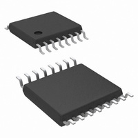
IC REG SW 1.5A W/SLEEP 16-TSSOP
Manufacturer
National Semiconductor
Series
PowerWise®r
Type
Step-Down (Buck)r
Datasheet
1.LM26001QMXANOPB.pdf
(18 pages)
Specifications of LM26001QMXAX/NOPB
Internal Switch(s)
Yes
Synchronous Rectifier
No
Number Of Outputs
1
Voltage - Output
1.25 ~ 35 V
Current - Output
1.5A
Frequency - Switching
150kHz ~ 500kHz
Voltage - Input
4 ~ 38 V
Operating Temperature
-40°C ~ 125°C
Mounting Type
Surface Mount
Package / Case
16-TSSOP Exposed Pad, 16-eTSSOP, 16-HTSSOP
Power - Output
2.6W
Lead Free Status / RoHS Status
Lead free / RoHS Compliant
Other names
LM26001QMXAX
Available stocks
Company
Part Number
Manufacturer
Quantity
Price
Company:
Part Number:
LM26001QMXAX/NOPB
Manufacturer:
MOLEX
Quantity:
10 000
helpful in short circuit conditions, when inductor current can
rise very high during the minimum on-time. Frequency reduc-
tion begins at 20% below the nominal frequency setting. The
minimum operating frequency in foldback mode is 71 kHz
typical.
If the FB voltage falls below the frequency foldback threshold
during frequency synchronized operation, the SYNC function
is disabled. Operating frequency versus FB voltage in short
circuit conditions is shown in the typical performance charac-
teristics section.
In conditions where the on time is close to minimum (less than
200nsec typically), such as high input voltage and high
switching frequency, the current limit may not function prop-
erly. This is because the current limit circuit cannot reduce the
on-time below minimum which prevents entry into frequency
foldback mode. There are two ways to ensure proper current
limit and foldback operation under high input voltage condi-
tions. First, the operating frequency can be reduced to in-
crease the nominal on time. Second, the inductor value can
be increased to slow the current ramp and reduce the peak
over-current.
FREQUENCY ADJUSTMENT AND SYNCHRONIZATION
The switching frequency of the LM26001 can be adjusted be-
tween 150 kHz and 500 kHz using a single external resistor.
This resistor is connected from the FREQ pin to ground as
shown in the typical application. The resistor value can be
calculated with the following empirically derived equation:
The switching frequency can also be synchronized to an ex-
ternal clock signal using the SYNC pin. The SYNC pin allows
the operating frequency to be varied above and below the
nominal frequency setting. The adjustment range is from 30%
above nominal to 20% below nominal. External synchroniza-
tion requires a 1.2V (typical) peak signal level at the SYNC
pin. The FREQ resistor must always be connected to initialize
the nominal operating frequency. The operating frequency is
synchronized to the falling edge of the SYNC input. When
SYNC goes low, the high-side switch turns on. This allows
any duty cycle to be used for the sync signal when synchro-
nizing to a frequency higher than nominal. When synchroniz-
ing to a lower frequency, however, there is a minimum duty
cycle requirement for the SYNC signal, given in the equation
below:
FIGURE 5. Swtiching Frequency vs R
R
FREQ
= (6.25 x 10
10
) x f
SW
-1.042
FREQ
20179451
11
Where fnom is the nominal switching frequency set by the
FREQ resistor, and fsync is a square wave. If the SYNC pin
is not used, it must be pulled low for normal operation. A
10kΩ pull-down resistor is recommended to protect against a
missing sync signal. Although the LM26001 is designed to
operate at up to 500 kHz, maximum load current may be lim-
ited at higher frequencies due to increased temperature rise.
See the Thermal Considerations section.
VBIAS
The VBIAS pin is used to bypass the internal regulator which
provides the bias voltage to the LM26001. When the VBIAS
pin is connected to a voltage greater than 3V, the internal
regulator automatically switches over to the VBIAS input. This
reduces the current into VIN (Iq) and increases system effi-
ciency. Using the VBIAS pin has the added benefit of reducing
power dissipation within the device.
For most applications where 3V < Vout < 10V, VBIAS can be
connected to Vout. If not used, VBIAS should be tied to GND.
If VBIAS drops below 2.9V (typical), the device automatically
switches over to supply the internal bias voltage from Vin.
LOW VIN OPERATION AND UVLO
The LM26001 is designed to remain operational during short
line transients when input voltage may drop as low as 3.0V.
Minimum nominal operating input voltage is 4.0V. Below this
voltage, switch R
voltage from VDD. The minimum voltage required at VDD is
approximately 3.5V for normal operation within specification.
VDD can also be used as a pull-up voltage for functions such
as PGOOD and FPWM. Note that if VDD is used externally,
the pin is not recommended for loads greater than 1 mA.
If the input voltage approaches the nominal output voltage,
the duty cycle is maximized to hold up the output voltage. In
this mode of operation, once the duty cycle reaches its max-
imum, the LM26001 can skip a maximum of seven off pulses,
effectively increasing the duty cycle and thus minimizing the
dropout from input to output. Typical off-pulse skipping wave-
forms are shown below.
UVLO is sensed at both VIN and VDD, and is activated when
either voltage falls below 2.9V (typical). Although VDD is typ-
FIGURE 6. Off-pulse Skipping Waveforms
Vin = 3.5V, Vnom = 3.3V, fnom = 305kHz
DS(ON)
increases, due to the lower gate drive
20179429
www.national.com


