LM26001QMXAX/NOPB National Semiconductor, LM26001QMXAX/NOPB Datasheet - Page 3
LM26001QMXAX/NOPB
Manufacturer Part Number
LM26001QMXAX/NOPB
Description
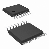
IC REG SW 1.5A W/SLEEP 16-TSSOP
Manufacturer
National Semiconductor
Series
PowerWise®r
Type
Step-Down (Buck)r
Datasheet
1.LM26001QMXANOPB.pdf
(18 pages)
Specifications of LM26001QMXAX/NOPB
Internal Switch(s)
Yes
Synchronous Rectifier
No
Number Of Outputs
1
Voltage - Output
1.25 ~ 35 V
Current - Output
1.5A
Frequency - Switching
150kHz ~ 500kHz
Voltage - Input
4 ~ 38 V
Operating Temperature
-40°C ~ 125°C
Mounting Type
Surface Mount
Package / Case
16-TSSOP Exposed Pad, 16-eTSSOP, 16-HTSSOP
Power - Output
2.6W
Lead Free Status / RoHS Status
Lead free / RoHS Compliant
Other names
LM26001QMXAX
Available stocks
Company
Part Number
Manufacturer
Quantity
Price
Company:

Part Number:
LM26001QMXAX/NOPB
Manufacturer:
MOLEX
Quantity:
10 000


Absolute Maximum Ratings
If Military/Aerospace specified devices are required,
please contact the National Semiconductor Sales Office/
Distributors for availability and specifications.
Electrical Characteristics
over the junction temperature (T
guaranteed through test, design, or statistical correlation. Typical values represent the most likely parametric norm at T
and are provided for reference purposes only.
Voltages from the indicated pins to GND:
VIN
SW
VDD
VBIAS
FB
BOOT
PGOOD
FREQ
SYNC
EN
FPWM
System
I
Iq
Iq
Iq
Iq
I
I
V
I
ΔV
ΔV
VDD
I
V
Switching
R
I
f
V
f
V
I
F
SD
BIAS_Sleep
BIAS_PWM
FB
SS_Source
sw_off
sw
SW
SYNC
FB
bias_th
FREQ
SYNC
SYNC_UP
DS(ON)
_Sleep_VB
_Sleep_VDD
_PWM_VB
_PWM_VDD
OUT
OUT
(Note
range
(Note
Symbol
/ΔV
/ΔI
OUT
6)
(Note
IN
7)
(Note
6)
6)
Shutdown Current
Quiescent Current
Quiescent Current
Quiescent Current
Quiescent Current
Bias Current
Bias Current
Feedback Voltage
FB Bias Current
Vout line regulation
Vout load regulation
VDD output voltage
Soft-start source current
VBIAS On Voltage
Switch on Resistance
Switch off state leakage current
Switching Frequency
FREQ voltage
Switching Frequency range
Sync pin threshold
Sync pin hysteresis
SYNC leakage current
Upper frequency synchronization
range
-0.3V to 40V
-0.5V to 40V
-0.3V to 7V
-0.3V to 10V
-0.3V to 6V
SW-0.3V to SW+7V
-0.3V to 7V
-0.3V to 7V
-0.3V to 7V
-0.3V to 40V
-0.3V to 7V
J
) range of -40°C to +125°C. Unless otherwise stated, Vin=12V. Minimum and Maximum limits are
Parameter
Specifications in standard type are for T
(Note
(Note
5)
1)
EN = 0V
Sleep mode, VBIAS = 5V
Sleep mode, VBIAS = GND
PWM mode, VBIAS = 5V
PWM mode, VBIAS = GND
Sleep mode, VBIAS = 5V
PWM mode, VBIAS = 5V
5V < Vin < 38V
5V < Vin <38V
0.8V < V
7V < Vin < 35V, I
mA
Specified at I
value
Isw = 1A
Vin = 38V, VSW = 0V
RFREQ = 62k, 124k, 240k
SYNC rising
SYNC falling
As compared to nominal f
3
Operating Ratings
SS
Storage Temperature
Power Dissipation (Note 2)
Recommended Lead
Temperature
ESD Susceptibility (Note 3)
Operating Junction Temp.
Supply Voltage
COMP
Conditions
Vapor Phase (70s)
Infrared (15s)
Machine Model
Human Body Model
Charged Device Model
BIAS
< 1.15V
VDD
= 92.5% of full
= 0 mA to 5
J
(Note
= 25°C only, and limits in boldface type apply
SW
4)
1.2155
5.50
2.64
0.12
Min
150
1.5
0.8
-0.3V to 7V
-65°C to +150°C
2.6 W
215°C
220°C
200V
2KV
1kV
(Note
1.234
0.001
0.002
10.8
0.65
0.07
5.95
Typ
150
114
0.5
2.2
2.9
0.2
1.0
1.2
1.1
38
75
33
6
1)
−40°C to 125°C
1.2525
±200
Max
0.85
0.70
6.50
3.07
0.42
125
230
±10
500
+30
4.6
5.0
1.6
20
70
85
3.0V to 38V
www.national.com
J
= 25°C,
Unit
%/V
kHz
mA
mA
mV
µA
µA
µA
µA
µA
nA
µA
µA
nA
%
%
%
Ω
V
V
V
V
V
Related parts for LM26001QMXAX/NOPB
Image
Part Number
Description
Manufacturer
Datasheet
Request
R

Part Number:
Description:
National Semiconductor [8-Bit D/A Converter]
Manufacturer:
National Semiconductor
Datasheet:
Part Number:
Description:
National Semiconductor [Media Coprocessor]
Manufacturer:
National Semiconductor
Datasheet:
Part Number:
Description:
Digitally Controlled Tone and Volume Circuit with Stereo Audio Power Amplifier, Microphone Preamp Stage and National 3D Sound
Manufacturer:
National Semiconductor
Datasheet:
Part Number:
Description:
Digitally Controlled Tone and Volume Circuit with Stereo Audio Power Amplifier, Microphone Preamp Stage and National 3D Sound
Manufacturer:
National Semiconductor
Datasheet:
Part Number:
Description:
AC97 Rev 2 Codec with Sample Rate Conversion and National 3D Sound
Manufacturer:
National Semiconductor
Part Number:
Description:
Manufacturer:
National Semiconductor
Datasheet:
Part Number:
Description:
Manufacturer:
National Semiconductor
Datasheet:
Part Number:
Description:
General Purpose, Low Voltage, Low Power, Rail-to-Rail Output Operational Amplifiers
Manufacturer:
National Semiconductor
Datasheet:
Part Number:
Description:
8-bit 20 MSPS flash A/D converter.
Manufacturer:
National Semiconductor
Datasheet:
Part Number:
Description:
Low Noise Quad Operational Amplifier
Manufacturer:
National Semiconductor
Datasheet:
Part Number:
Description:
Quad Differential Line Receivers
Manufacturer:
National Semiconductor
Datasheet:
Part Number:
Description:
Quad High Speed Trapezoidal? Bus Transceiver
Manufacturer:
National Semiconductor
Datasheet:
Part Number:
Description:
Dual Line Receiver
Manufacturer:
National Semiconductor
Datasheet:
Part Number:
Description:
TTL to 10k ECL Level Translator with Latch
Manufacturer:
National Semiconductor
Datasheet: