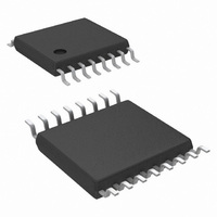
LM26001QMXAX/NOPB National Semiconductor, LM26001QMXAX/NOPB Datasheet - Page 12

LM26001QMXAX/NOPB
Manufacturer Part Number
LM26001QMXAX/NOPB
Description
IC REG SW 1.5A W/SLEEP 16-TSSOP
Manufacturer
National Semiconductor
Series
PowerWise®r
Type
Step-Down (Buck)r
Datasheet
1.LM26001QMXANOPB.pdf
(18 pages)
Specifications of LM26001QMXAX/NOPB
Internal Switch(s)
Yes
Synchronous Rectifier
No
Number Of Outputs
1
Voltage - Output
1.25 ~ 35 V
Current - Output
1.5A
Frequency - Switching
150kHz ~ 500kHz
Voltage - Input
4 ~ 38 V
Operating Temperature
-40°C ~ 125°C
Mounting Type
Surface Mount
Package / Case
16-TSSOP Exposed Pad, 16-eTSSOP, 16-HTSSOP
Power - Output
2.6W
Lead Free Status / RoHS Status
Lead free / RoHS Compliant
Other names
LM26001QMXAX
Available stocks
Company
Part Number
Manufacturer
Quantity
Price
Company:
Part Number:
LM26001QMXAX/NOPB
Manufacturer:
MOLEX
Quantity:
10 000
www.national.com
ically less than 200mV below VIN, it will not discharge through
VIN. Therefore when the VIN voltage drops rapidly, VDD may
remain high, especially in sleep mode. For fast line voltage
transients, using a larger capacitor at the VDD pin can help
to hold off a UVLO shutdown by extending the VDD discharge
time. By holding up VDD, a larger cap can also reduce the
R
nately, under heavy loading the VDD voltage can fall several
hundred mV below VIN. In this case, UVLO may be triggered
by VDD even though the VIN voltage is above the UVLO
threshold.
When UVLO is activated the LM26001 enters a standby state
in which VDD remains charged. As input voltage and VDD
voltage rise above 3.9V (typical) the device will restart from
softstart mode.
PGOOD
A power good pin, PGOOD, is available to monitor the output
voltage status. The pin is internally connected to an open
SETTING OUTPUT VOLTAGE
The output voltage is set by the ratio of a voltage divider at
the FB pin as shown in the typical application. The resistor
values can be determined by the following equation:
Where Vfb = 1.234V typically.
A maximum value of 150kΩ is recommended for the sum of
R1 and R2.
As input voltage decreases towards the nominal output volt-
age, the LM26001 can skip up to seven off-pulses as de-
scribed in the Low Vin Operation section. In low output voltage
applications, if the on-time reaches Ton
skip on-pulses to maintain regulation. There is no limit to the
number of pulses that are skipped. In this mode of operation,
however, output ripple voltage may increase slightly.
DS(ON)
(and dropout voltage) in low VIN conditions. Alter-
MIN
, the device will
FIGURE 7. Example Circuit
1.5A Max, 305 kHz
12
drain MOSFET, which remains open while the output voltage
is within operating range. PGOOD goes low (low impedance
to ground) when the output falls below 85% of nominal or EN
is pulled low. When the output voltage returns to within 92%
of nominal, as measured at the FB pin, PGOOD returns to a
high state. For improved noise immunity, there is a 5us delay
between the PGOOD threshold and the PGOOD pin going
low.
Design Information
EXAMPLE CIRCUIT
Figure 7 shows a complete typical application schematic. The
components have been selected based on the design criteria
given in the following sections.
INDUCTOR
The output inductor should be selected based on inductor
ripple current. The amount of inductor ripple current com-
pared to load current, or ripple content, is defined as Iripple/
Iload. Ripple content should be less than 40%. Inductor ripple
current, Iripple, can be calculated as shown below:
Larger ripple content increases losses in the inductor and re-
duces the effective current limit.
Larger inductance values result in lower output ripple voltage
and higher efficiency, but a slightly degraded transient re-
sponse. Lower inductance values allow for smaller case size,
but the increased ripple lowers the effective current limit
threshold.
Remember that inductor value also affects the sleep mode
threshold as shown in Figure 3.
20179430


