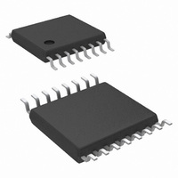
LM26001QMXAX/NOPB National Semiconductor, LM26001QMXAX/NOPB Datasheet - Page 14

LM26001QMXAX/NOPB
Manufacturer Part Number
LM26001QMXAX/NOPB
Description
IC REG SW 1.5A W/SLEEP 16-TSSOP
Manufacturer
National Semiconductor
Series
PowerWise®r
Type
Step-Down (Buck)r
Datasheet
1.LM26001QMXANOPB.pdf
(18 pages)
Specifications of LM26001QMXAX/NOPB
Internal Switch(s)
Yes
Synchronous Rectifier
No
Number Of Outputs
1
Voltage - Output
1.25 ~ 35 V
Current - Output
1.5A
Frequency - Switching
150kHz ~ 500kHz
Voltage - Input
4 ~ 38 V
Operating Temperature
-40°C ~ 125°C
Mounting Type
Surface Mount
Package / Case
16-TSSOP Exposed Pad, 16-eTSSOP, 16-HTSSOP
Power - Output
2.6W
Lead Free Status / RoHS Status
Lead free / RoHS Compliant
Other names
LM26001QMXAX
Available stocks
Company
Part Number
Manufacturer
Quantity
Price
Company:
Part Number:
LM26001QMXAX/NOPB
Manufacturer:
MOLEX
Quantity:
10 000
www.national.com
A Schottky diode must be used. It's low forward voltage max-
imizes efficiency and BOOT voltage, while also protecting the
SW pin against large negative voltage spikes
COMPENSATION
The purpose of loop compensation is to ensure stable oper-
ation while maximizing dynamic performance. Stability can be
analyzed with loop gain measurements, while dynamic per-
formance is analyzed with both loop gain and load transient
response. Loop gain is equal to the product of control-output
transfer function (power stage) and the feedback transfer
function (the compensation network).
For stability purposes, our target is to have a loop gain slope
that is -20dB /decade from a very low frequency to beyond
the crossover frequency. Also, the crossover frequency
should not exceed one-fifth of the switching frequency, i.e. 60
kHz in the case of 300 kHz switching frequency.
For dynamic purposes, the higher the bandwidth, the faster
the load transient response. A large DC gain means high DC
regulation accuracy (i.e. DC voltage changes little with load
or line variations). To achieve this loop gain, the compensa-
tion components should be set according to the shape of the
control-output bode plot. A typical plot is shown in Figure 8
below.
The control-output transfer function consists of one pole (fp),
one zero (fz), and a double pole at fn (half the switching fre-
quency).
Referring to Figure 8, the following should be done to create
a -20dB /decade roll-off of the loop gain:
1. Place a pole at 0Hz (fpc)
2. Place a zero at fp (fzc)
3. Place a second pole at fz (fpc1)
The resulting feedback (compensation) bode plot is shown
below in Figure 9. Adding the control-output response to the
feedback response will then result in a nearly continuous
-20db/decade slope.
FIGURE 8. Control-Output Transfer Function
20179438
14
The control-output corner frequencies can be determined ap-
proximately by the following equations:
Where Co is the output capacitance, Ro is the load resistance,
Re is the output capacitor ESR, and fsw is the switching fre-
quency. The effects of slope compensation and current sense
gain are included in this equation. However, the equation is
an approximation intended to simplify loop compensation cal-
culations. To derive the exact transfer function, use 0.2V/V
sense amp gain and 36mVp-p slope compensation.
Since fp is determined by the output network, it shifts with
loading. Determine the range of frequencies (fpmin/max)
across the expected load range. Then determine the com-
pensation values as described below and shown in Figure 10.
1. The compensation network automatically introduces a low
frequency pole (fpc), which is close to 0Hz.
2. Once the fp range is determined, R5 should be calculated
using:
FIGURE 9. Feedback Transfer Function
FIGURE 10. Compensation Network
20179443
20179439


