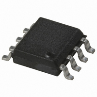
HCPL-0710 Avago Technologies US Inc., HCPL-0710 Datasheet - Page 6

HCPL-0710
Manufacturer Part Number
HCPL-0710
Description
OPTOCOUPLER CMOS 12MBD 8-SOIC
Manufacturer
Avago Technologies US Inc.
Datasheet
1.HCPL-7710-000E.pdf
(18 pages)
Specifications of HCPL-0710
Voltage - Isolation
3750Vrms
Number Of Channels
1, Unidirectional
Current - Output / Channel
10mA
Data Rate
12.5MBd
Propagation Delay High - Low @ If
20ns
Input Type
Logic
Output Type
Push-Pull, Totem-Pole
Mounting Type
Surface Mount
Package / Case
8-SOIC (0.154", 3.90mm Width)
No. Of Channels
1
Isolation Voltage
3.75kV
Optocoupler Output Type
Gate Drive
Input Current
10µA
Output Voltage
5V
Opto Case Style
SOIC
No. Of Pins
8
Propagation Delay Low-high
40ns
Common Mode Voltage Vcm
1000V
Lead Free Status / RoHS Status
Contains lead / RoHS non-compliant
Other names
516-1116-5
Available stocks
Company
Part Number
Manufacturer
Quantity
Price
Company:
Part Number:
HCPL-0710
Manufacturer:
AVAGO
Quantity:
18 000
Part Number:
HCPL-0710
Manufacturer:
AGILENT
Quantity:
20 000
Company:
Part Number:
HCPL-0710#000E
Manufacturer:
AVAGO
Quantity:
30 000
Company:
Part Number:
HCPL-0710#500
Manufacturer:
AGILENT
Quantity:
1 726
Company:
Part Number:
HCPL-0710#500E
Manufacturer:
AVAGO
Quantity:
21 000
Company:
Part Number:
HCPL-0710-000E
Manufacturer:
AVAGO
Quantity:
30 000
Part Number:
HCPL-0710-500
Manufacturer:
AVAGO/安华高
Quantity:
20 000
Part Number:
HCPL-0710-500E
Manufacturer:
AVAGO/安华高
Quantity:
20 000
6
IEC/EN/DIN EN 60747-5-2 Insulation Related Characteristics (Option 060)
†Refer to the front of the optocoupler section of the Isolation and Control Component Designer’s Catalog, under Product Safety Regulations sec-
tion IEC/EN/DIN EN 60747-5-2, for a detailed description.
Note: These optocouplers are suitable for “safe electrical isolation” only within the safety limit data. Maintenance of the safety data shall be
Note: The surface mount classification is Class A in accordance with CECC 00802.
Absolute Maximum Ratings
Recommended Operating Conditions
Description
Installation classification per DIN VDE 0110/1.89, Table 1
Climatic Classification
Pollution Degree (DIN VDE 0110/1.89)
Maximum Working Insulation Voltage
Input to Output Test Voltage, Method b†
Input to Output Test Voltage, Method a†
Highest Allowable Overvoltage†
(Transient Overvoltage, t
Safety Limiting Values
Insulation Resistance at T
Parameter
Storage Temperature
Ambient Operating Temperature
Supply Voltages
Input Voltage
Output Voltage
Input Current
Average Output Current
Lead Solder Temperature
Solder Reflow Temperature Profile
Parameter
Ambient Operating Temperature
Supply Voltages
Logic High Input Voltage
Logic Low Input Voltage
Input Signal Rise and Fall Times
V
Test with t
V
for rated mains voltage ≤150 V rms
for rated mains voltage ≤300 V rms
for rated mains voltage ≤450 V rms
t
(Maximum values allowed in the event of a failure,
also see Thermal Derating curve, Figure 11.)
m
IORM
IORM
Case Temperature
Input Current
Output Power
ensured by means of protective circuits.
= 60 sec, Partial Discharge < 5 pC
x 1.875 = V
x 1.5 = V
m
= 1 sec, Partial Discharge < 5 pC
PR
, Type and Sample Test,
PR
, 100% Production
ini
S
, V
= 10 sec)
10
= 500 V
Symbol
V
V
V
V
T
I
P
R
Symbol
T
T
V
V
V
I
I
260°C for 10 sec., 1.6 mm below seating plane
See Solder Reflow Temperature Profile Section
Symbol
T
V
V
V
t
S,INPUT
I
O
r
A
A
IORM
I
O
DD1
IH
IL
S
S,OUTPUT
IO
S
, t
PR
PR
IOTM
DD1
f
, V
, V
DD2
DD2
HCPL-7710
Option 060
I-III
55/100/21
2
630
1181
945
6000
175
230
600
≥10
Min.
–40
4.5
2.0
0.0
Min.
–55
–40
0
–0.5
–0.5
–10
I-IV
I-IV
9
HCPL-0710
Option 060
55/100/21
2
560
1050
840
4000
150
150
600
≥10
Max.
125
+100
6.0
V
V
+10
10
Max.
+100
5.5
V
0.8
1.0
I-IV
I-III
DD2
DD1
DD1
9
+0.5
+0.5
Units
V peak
V peak
V peak
V peak
°C
mA
mW
Ω
Units
°C
°C
Volts
Volts
Volts
mA
mA
Units
°C
V
V
V
ms


