SPDC12L00010 STMicroelectronics, SPDC12L00010 Datasheet - Page 21
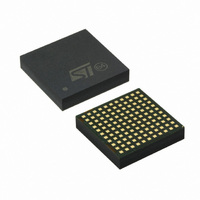
SPDC12L00010
Manufacturer Part Number
SPDC12L00010
Description
IC BUCK ADJ 10A 121LGA
Manufacturer
STMicroelectronics
Type
Point of Load (POL) Non-Isolated with UVLOr
Datasheet
1.SPDC12L00010.pdf
(29 pages)
Specifications of SPDC12L00010
Output
0.6 ~ 5V
Number Of Outputs
1
Power (watts)
50W
Mounting Type
Surface Mount
Voltage - Input
1.8 ~ 14V
Package / Case
121-LGA
1st Output
0.6 ~ 5 VDC @ 10A
Size / Dimension
0.59" L x 0.59" W x 0.11" H (15mm x 15mm x 2.8mm)
Power (watts) - Rated
50W
Operating Temperature
-40°C ~ 85°C
Efficiency
93%
Current - Output
10A
Voltage - Output
0.6 ~ 5 V
Frequency - Switching
729kHz
Synchronous Rectifier
No
Output Voltage
0.6 V to 5 V
Output Current
0 A to 10 A
Input Voltage
1.8 V to 14 V
Supply Current
65 mA
Switching Frequency
729 KHz
Maximum Operating Temperature
+ 85 C
Minimum Operating Temperature
- 40 C
Lead Free Status / RoHS Status
Lead free / RoHS Compliant
3rd Output
-
2nd Output
-
Lead Free Status / Rohs Status
Lead free / RoHS Compliant
Other names
497-9072
Available stocks
Company
Part Number
Manufacturer
Quantity
Price
Company:

Part Number:
SPDC12L00010
Manufacturer:
ADI
Quantity:
13


SPDC12L00010
5.12
5.13
Figure 6.
Output voltage programming
Adding a resistor Rx between FB (pin L9) and SGND (L8) or between FB and VSENSE (pin
L2), it is possible to change the output voltage.
Connecting the resistor to SGND the output voltage increase (see
Connecting the resistor to VSENSE the output voltage decrease (see
Calculate the resistor for increasing output voltage with the following formula:
R
Calculate the resistor for decreasing output voltage with the following formula:
R
The module output voltage is 1.2 V with R
Figure 7.
Additional loop compensation
If required by particular load condition, it is possible to change the feedback loop
compensation, adding a pole with an external R-C network between FB (pin L9) and COMP
(pin L10) (see
VSENSE (pin L2) (see
x
x
= 0.6 / (V
= (V
OUT
– 0.6) / (1.2 – V
OUT
Voltage sensing
Output voltage programming
Figure 8
– 1.2)
Figure 8
a), or adding a zero with an external R-C network between FB and
[kΩ] valid for V
OUT
Doc ID 15103 Rev 3
) [kΩ] valid for 0.6 < V
b).
OUT
x
= n.c.
> 1.2 V
OUT
< 1.2 V
Application information
Figure 7
Figure 7
a);
b).
21/29
Related parts for SPDC12L00010
Image
Part Number
Description
Manufacturer
Datasheet
Request
R

Part Number:
Description:
STMicroelectronics [RIPPLE-CARRY BINARY COUNTER/DIVIDERS]
Manufacturer:
STMicroelectronics
Datasheet:
Part Number:
Description:
STMicroelectronics [LIQUID-CRYSTAL DISPLAY DRIVERS]
Manufacturer:
STMicroelectronics
Datasheet:

Part Number:
Description:
BOARD EVAL FOR MEMS SENSORS
Manufacturer:
STMicroelectronics
Datasheet:
Part Number:
Description:
NPN TRANSISTOR POWER MODULE
Manufacturer:
STMicroelectronics
Datasheet:
Part Number:
Description:
TURBOSWITCH ULTRA-FAST HIGH VOLTAGE DIODE
Manufacturer:
STMicroelectronics
Datasheet:
Part Number:
Description:
Manufacturer:
STMicroelectronics
Datasheet:
Part Number:
Description:
DIODE / SCR MODULE
Manufacturer:
STMicroelectronics
Datasheet:
Part Number:
Description:
DIODE / SCR MODULE
Manufacturer:
STMicroelectronics
Datasheet:
Part Number:
Description:
Search -----> STE16N100
Manufacturer:
STMicroelectronics
Datasheet:
Part Number:
Description:
Search ---> STE53NA50
Manufacturer:
STMicroelectronics
Datasheet:
Part Number:
Description:
NPN Transistor Power Module
Manufacturer:
STMicroelectronics
Datasheet:
Part Number:
Description:
DIODE / SCR MODULE
Manufacturer:
STMicroelectronics
Datasheet: