SPDC12L00010 STMicroelectronics, SPDC12L00010 Datasheet - Page 23
SPDC12L00010
Manufacturer Part Number
SPDC12L00010
Description
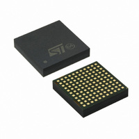
IC BUCK ADJ 10A 121LGA
Manufacturer
STMicroelectronics
Type
Point of Load (POL) Non-Isolated with UVLOr
Datasheet
1.SPDC12L00010.pdf
(29 pages)
Specifications of SPDC12L00010
Output
0.6 ~ 5V
Number Of Outputs
1
Power (watts)
50W
Mounting Type
Surface Mount
Voltage - Input
1.8 ~ 14V
Package / Case
121-LGA
1st Output
0.6 ~ 5 VDC @ 10A
Size / Dimension
0.59" L x 0.59" W x 0.11" H (15mm x 15mm x 2.8mm)
Power (watts) - Rated
50W
Operating Temperature
-40°C ~ 85°C
Efficiency
93%
Current - Output
10A
Voltage - Output
0.6 ~ 5 V
Frequency - Switching
729kHz
Synchronous Rectifier
No
Output Voltage
0.6 V to 5 V
Output Current
0 A to 10 A
Input Voltage
1.8 V to 14 V
Supply Current
65 mA
Switching Frequency
729 KHz
Maximum Operating Temperature
+ 85 C
Minimum Operating Temperature
- 40 C
Lead Free Status / RoHS Status
Lead free / RoHS Compliant
3rd Output
-
2nd Output
-
Lead Free Status / Rohs Status
Lead free / RoHS Compliant
Other names
497-9072
Available stocks
Company
Part Number
Manufacturer
Quantity
Price
Company:

Part Number:
SPDC12L00010
Manufacturer:
ADI
Quantity:
13


SPDC12L00010
5.16
5.17
5.18
5.19
Thermal shutdown
When the controller junction temperature reaches 150 ± 10 °C, the device shutdown.
Both MOSFET are turned OFF and the soft-start capacitor is discharged.
The device does not restart until the junction temperature goes down to 120 °C and until the
voltage on the soft-start capacitor reaches 0.5 V.
Signal ground and power ground
SGND (L8) and PGND (bank 2) are connected together on the module.
Connect to SGND the capacitor for PGDLY and SS_INL, the resistor for FB and OS.
Connect to PGND the return for SS_INL.
It is important to not create a ground loop between SGND, PGND and other GND present on
the application circuit (see
Figure 9.
Input capacitors
The input capacitor present on the module is not able to sustain the input RMS current.
Connect 2 x 2.2 μF 16 V X7R ceramic capacitor (Cin) closed to the input pins VIN and
PGND (bank 1 and bank 2), to satisfy minimum functional requirement.
Connect proper low impedance capacitors to reduce the input ripple current, according to
the application requirement.
Output capacitors
The output capacitors present on the module are able to sustain output RMS current.
Connect 2 x 330 μF POSCAP SANYO capacitor (Co) or equivalent, closed to the output pins
VOUT and PGND (bank 3 and bank 2), to guarantee output voltage stability and specified
voltage ripple.
Signal ground and power ground
Figure
Doc ID 15103 Rev 3
9).
Application information
23/29
Related parts for SPDC12L00010
Image
Part Number
Description
Manufacturer
Datasheet
Request
R

Part Number:
Description:
STMicroelectronics [RIPPLE-CARRY BINARY COUNTER/DIVIDERS]
Manufacturer:
STMicroelectronics
Datasheet:
Part Number:
Description:
STMicroelectronics [LIQUID-CRYSTAL DISPLAY DRIVERS]
Manufacturer:
STMicroelectronics
Datasheet:

Part Number:
Description:
BOARD EVAL FOR MEMS SENSORS
Manufacturer:
STMicroelectronics
Datasheet:
Part Number:
Description:
NPN TRANSISTOR POWER MODULE
Manufacturer:
STMicroelectronics
Datasheet:
Part Number:
Description:
TURBOSWITCH ULTRA-FAST HIGH VOLTAGE DIODE
Manufacturer:
STMicroelectronics
Datasheet:
Part Number:
Description:
Manufacturer:
STMicroelectronics
Datasheet:
Part Number:
Description:
DIODE / SCR MODULE
Manufacturer:
STMicroelectronics
Datasheet:
Part Number:
Description:
DIODE / SCR MODULE
Manufacturer:
STMicroelectronics
Datasheet:
Part Number:
Description:
Search -----> STE16N100
Manufacturer:
STMicroelectronics
Datasheet:
Part Number:
Description:
Search ---> STE53NA50
Manufacturer:
STMicroelectronics
Datasheet:
Part Number:
Description:
NPN Transistor Power Module
Manufacturer:
STMicroelectronics
Datasheet:
Part Number:
Description:
DIODE / SCR MODULE
Manufacturer:
STMicroelectronics
Datasheet: