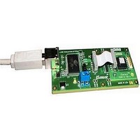
ADIS16265/PCBZ Analog Devices Inc, ADIS16265/PCBZ Datasheet - Page 10
ADIS16265/PCBZ
Manufacturer Part Number
ADIS16265/PCBZ
Description
BOARD EVALUATION FOR ADIS16265
Manufacturer
Analog Devices Inc
Series
iMEMS®, iSensor™r
Datasheet
1.ADIS16260PCBZ.pdf
(20 pages)
Specifications of ADIS16265/PCBZ
Sensor Type
Gyroscope, 1 Axis
Sensing Range
±80°/sec, ±160°/sec, ±320°/sec
Sensitivity
±0.2%
Embedded
No
Utilized Ic / Part
ADIS16265
Silicon Manufacturer
Analog Devices
Application Sub Type
Angular Rate Sensor / Gyroscope
Kit Application Type
Sensing - Motion / Vibration / Shock
Silicon Core Number
ADIS16265
Lead Free Status / RoHS Status
Lead free / RoHS compliant by exemption
Voltage - Supply
-
Interface
-
Lead Free Status / RoHS Status
Lead free / RoHS compliant by exemption


ADIS16260/ADIS16265
BASIC OPERATION
The ADIS16260 and ADIS16265 require only power, ground,
and the four SPI signals to produce data and make it available
to an embedded processor. Figure 9 provides a schematic for
connecting the ADIS16260 and ADIS16265 to a SPI-compatible
processor and includes one of the configurable digital I/O lines.
The MSC_CTRL[2:0] bits are used to configure this line as a data
ready indicator (see the Data Ready I/O Indicator section).
Table 5. Generic Master Processor Pin Names and Functions
Pin Name
SS
IRQ
MOSI
MISO
SCLK
PROCESSOR
SPI MASTER
SYSTEM
V
DD
INPUT/OUTPUT LINES ARE COMPATIBLE
DOUT
SCLK
NOTES
1. DOUT BITS ARE BASED ON THE PREVIOUS 16-BIT SEQUENCE (R/W = 0).
Figure 9. Electrical Connection Diagram
DIN
CS
WITH 3.3V OR 5V LOGIC LEVELS
SCLK
MOSI
MISO
IRQ
SS
DB15
Function
Slave select
Interrupt request input
Master output, slave input
Master input, slave output
Serial clock
R/W
DB14
A6
DB13
4
1
3
2
5
A5
CS
SCLK
DIN
DOUT
DIO1
DB12
A4
GND GND
VCC
ADIS16260/
ADIS16265
16
18
SPI SLAVE
DB11
A3
5V
VCC
17
19
DB10
A2
Figure 11. SPI Communication Bit Sequence
DB9
A1
DB8
A0
Rev. B | Page 10 of 20
DB7
D7
DB6
D6
DB5
D5
The ADIS16260 and ADIS16265 SPI interface supports full-
duplex serial communication (simultaneous transmit and
receive) and uses the bit sequence shown in Figure 11. Processor
platforms typically support SPI communication with general-
purpose serial ports that require some configuration in their
control registers. Table 6 provides a list of the most common
settings that require attention to initialize the serial port of a
processor for communication with the ADIS16260 and
ADIS16265.
Table 6. Generic Master Processor SPI Settings
Processor Setting
Master
SCLK Rate ≤ 2.5 MHz
SPI Mode 3
MSB First Mode
16-Bit Mode
User registers govern all data collection and configuration.
Table 7 provides a memory map that includes all user registers,
along with references to the bit assignment tables that follow the
generic bit assignments in Figure 10.
15
DB4
D4
14
DB3
D3
13
UPPER BYTE
DB2
12
D2
Figure 10. Generic Register Bit Definitions
11
DB1
D1
10
DB0
D0
Description
The ADIS16260 and ADIS16265 operate
as slaves
Bit rate setting (SMPL_PRD[7:0] ≤ 0x07)
Clock polarity, phase (CPOL = 1, CPHA = 1)
Bit sequence
Shift register/data length
9
8
DB15
7
R/W
6
DB14
A6
5
LOWER BYTE
DB13
A5
4
3
2
1
0
Related parts for ADIS16265/PCBZ
Image
Part Number
Description
Manufacturer
Datasheet
Request
R

Part Number:
Description:
±1.7g Dual-Axis IMEMS Accelerometer Evaluation Board
Manufacturer:
Analog Devices Inc
Datasheet:

Part Number:
Description:
Inertial Sensor Evaluation System
Manufacturer:
Analog Devices Inc
Datasheet:
Part Number:
Description:
Manufacturer:
Analog Devices Inc
Datasheet:
Part Number:
Description:
Manufacturer:
Analog Devices Inc
Datasheet:
Part Number:
Description:
Manufacturer:
Analog Devices Inc
Datasheet:
Part Number:
Description:
Manufacturer:
Analog Devices Inc
Datasheet:
Part Number:
Description:
Manufacturer:
Analog Devices Inc
Datasheet:
Part Number:
Description:
Manufacturer:
Analog Devices Inc
Datasheet:
Part Number:
Description:
Manufacturer:
Analog Devices Inc
Datasheet:
Part Number:
Description:
Manufacturer:
Analog Devices Inc
Datasheet:
Part Number:
Description:
Manufacturer:
Analog Devices Inc
Datasheet:
Part Number:
Description:
Manufacturer:
Analog Devices Inc
Datasheet:
Part Number:
Description:
Manufacturer:
Analog Devices Inc
Datasheet: