ADIS16265/PCBZ Analog Devices Inc, ADIS16265/PCBZ Datasheet - Page 18
ADIS16265/PCBZ
Manufacturer Part Number
ADIS16265/PCBZ
Description
BOARD EVALUATION FOR ADIS16265
Manufacturer
Analog Devices Inc
Series
iMEMS®, iSensor™r
Datasheet
1.ADIS16260PCBZ.pdf
(20 pages)
Specifications of ADIS16265/PCBZ
Sensor Type
Gyroscope, 1 Axis
Sensing Range
±80°/sec, ±160°/sec, ±320°/sec
Sensitivity
±0.2%
Embedded
No
Utilized Ic / Part
ADIS16265
Silicon Manufacturer
Analog Devices
Application Sub Type
Angular Rate Sensor / Gyroscope
Kit Application Type
Sensing - Motion / Vibration / Shock
Silicon Core Number
ADIS16265
Lead Free Status / RoHS Status
Lead free / RoHS compliant by exemption
Voltage - Supply
-
Interface
-
Lead Free Status / RoHS Status
Lead free / RoHS compliant by exemption


ADIS16260/ADIS16265
APPLICATIONS INFORMATION
ASSEMBLY
When developing a process flow for installing ADIS16260 and
ADIS16265 devices on PCBs, see the JEDEC standard document
J-STD-020C for reflow temperature profile and processing
information. The ADIS16260 and ADIS16265 can use the
Sn-Pb eutectic process and the Pb-free eutectic process from
this standard. See JEDEC J-STD-033 for moisture sensitivity
(MSL) handling requirements. The MSL rating for these devices
is marked on the antistatic bags, which protect these devices
from ESD during shipping and handling. Prior to assembly,
review the process flow for information about introducing
shock levels that exceed the absolute maximum ratings for the
ADIS16260 and ADIS16265. PCB separation and ultrasonic
cleaning processes can introduce high levels of shock and
damage the MEMS element. Bowing or flexing the PCB after
solder reflow can also place large pealing stress on the pad
structure and can damage the device. If this is unavoidable,
consider using an underfill material to help distribute these
forces across the bottom of the package. Figure 18 provides a
PCB pad design example for this package style.
BIAS OPTIMIZATION
Some environmental conditions, such as thermal cycling, can
influence the initial bias accuracy. Use the following steps to
fine-tune the bias after assembly to an accuracy that approaches
the in-run bias stability of 0.007°/sec.
1.
2.
Apply 5 V and wait 10 sec.
Set SENS_AVG[10:8] = 001 (DIN = 0xB901).
10.173
11mm × 11mm STACKED LGA PACKAGE
2×
Figure 18. Recommended Pad Layout (Units in Millimeters)
7.600
4×
3.800
8×
1.127
20×
5.0865
8×
0.773
0.500
16×
20×
Rev. B | Page 18 of 20
3.
4.
5.
6.
7.
8.
INTERFACE PRINTED CIRCUIT BOARD (PCB)
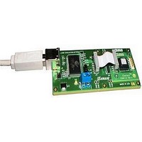
The ADIS16265/PCBZ includes one ADIS16265BCCZ IC on a
1.2 inch × 1.3 inch PCB. The ADIS16260/PCBZ includes one
ADIS16260BCCZ on a 1.2 inch × 1.3 inch PCB. The interface
PCB simplifies the IC connection of these devices to an existing
processor system. The four mounting holes accommodate either
M2 (2 mm) or 2-56 machine screws. These boards are made of
IS410 material and are 0.063 inches thick. The second-level
assembly uses a SAC305-compatible solder composition, which
has a presolder reflow thickness of approximately 0.005 inches.
The pad pattern on these PCBs matches that shown in Figure 20.
J1 and J2 are dual-row, 2 mm (pitch) connectors that work with
a number of ribbon cable systems, including 3M Part Number
152212-0100-GB (ribbon crimp connector) and 3M Part Number
3625/12 (ribbon cable). The schematic and connector pin
assignments for the ADIS16260/PCBZ and the ADIS16265/PCBZ
are shown in Figure 19.
Collect GYRO_OUT data for 150 sec at a sample rate of
256 SPS.
Average data record.
Round to the nearest integer.
Multiply by −1.
Write to GYRO_OFF.
Update flash.
Set GLOB_CMD[3] = 1 (DIN = 0xBE04).
Wait for >50 ms and resume operation.
C1
10
11
12
1
2
3
4
5
6
7
8
9
18
19
16
17
Figure 19. Electrical Schematic
7
1
4
2
3
RST
SCLK
CS
DOUT
DIN
GND
GND
VCC
VCC
14
ADIS16260/
RATE
ADIS16265
C2
FILT
AUX DAC
AUX ADC
15
VREF
DIO2
DIO1
13
12
20
6
5
10
11
12
1
2
3
4
5
6
7
8
9
Related parts for ADIS16265/PCBZ
Image
Part Number
Description
Manufacturer
Datasheet
Request
R

Part Number:
Description:
±1.7g Dual-Axis IMEMS Accelerometer Evaluation Board
Manufacturer:
Analog Devices Inc
Datasheet:

Part Number:
Description:
Inertial Sensor Evaluation System
Manufacturer:
Analog Devices Inc
Datasheet:
Part Number:
Description:
Manufacturer:
Analog Devices Inc
Datasheet:
Part Number:
Description:
Manufacturer:
Analog Devices Inc
Datasheet:
Part Number:
Description:
Manufacturer:
Analog Devices Inc
Datasheet:
Part Number:
Description:
Manufacturer:
Analog Devices Inc
Datasheet:
Part Number:
Description:
Manufacturer:
Analog Devices Inc
Datasheet:
Part Number:
Description:
Manufacturer:
Analog Devices Inc
Datasheet:
Part Number:
Description:
Manufacturer:
Analog Devices Inc
Datasheet:
Part Number:
Description:
Manufacturer:
Analog Devices Inc
Datasheet:
Part Number:
Description:
Manufacturer:
Analog Devices Inc
Datasheet:
Part Number:
Description:
Manufacturer:
Analog Devices Inc
Datasheet:
Part Number:
Description:
Manufacturer:
Analog Devices Inc
Datasheet: