CYII4SM6600-EVAL Cypress Semiconductor Corp, CYII4SM6600-EVAL Datasheet
CYII4SM6600-EVAL
Specifications of CYII4SM6600-EVAL


Related parts for CYII4SM6600-EVAL

CYII4SM6600-EVAL Summary of contents
Page 1
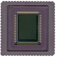
... MHz housed in a 68-pin ceramic LCC package. This data sheet enables you to develop a camera system, based on the described timing and interfacing given in the following sections. Figure 1. IBIS4-6600 Image Sensor • 198 Champion Court • San Jose IBIS4-6600 CYII4SM6600AB , CA 95134-1709 • 408-943-2600 Revised April 1,2010 [+] Feedback ...
Page 2
... Marketing Part Number CYII4SM6600AB-QDC Mono with Glass CYII4SM6600AB-QWC Mono without Glass CYII4SE6600AB-QDC Color micro lens with Glass CYII4SE6600AB-QFCH Color micro lens with IR Coating, High Grade CYII4SM6600-EVAL Mono Demo Kit CYII4SC6600-EVAL Color Demo Kit Specifications General Specifications Parameter Pixel Architecture 3T-Pixel Pixel Size 3.5 µ ...
Page 3
... The sensor is light sensitive between 400 and 1000 nm. The peak 25% approximately 650 nm. In view of a fill factor of 35%, the QE is close to 70% between 500 and 700 nm. Document Number: 001-02366 Rev. *G IBIS4-6600 CYII4SM6600AB Figure 2. Spectral Response Curve QE 20% ...
Page 4
... Mpixel/s Two on-chip 10-bit ADCs at 20 Msamples/s are multiplexed to one digital 10-bit output at 40 Msamples/s Nominal 2.5V (some supplies require 3.3V for extended dynamic range) 2.5V Serial-to Parallel Interface (SPI) 68-pins LCC IBIS4-6600 CYII4SM6600AB 20000 25000 Table 7 on page 12) Page [+] Feedback ...
Page 5
... GND. Condition Min V DD –0 GND – =min –100 =min 100 System clock <= 40 MHz 70 to analog circuit). DDA IBIS4-6600 CYII4SM6600AB Value Unit –0 ± 350 °C –30 to +85 °C 85 °C 2000 V Typ Max Unit 2.5 3 +65 °C ...
Page 6
... The start address is uploaded through the serial to parallel interface. Most of the signals for the image core shown in generated on-chip by the sequencer. This sequencer also allows running the sensor in basic modes, not fully autonomous. IBIS4-6600 CYII4SM6600AB addres s & data bus Dig. logic (2) ...
Page 7
... Document Number: 001-02366 Rev. *G IBIS4-6600 CYII4SM6600AB Color Filter Array The IBIS4-6600 can also be processed with a Bayer RGB color pattern. Pixel (0,0) has a green filter and is situated on a green-red row. Green1 and Green2 are separately processed color filters and have a different spectral response. Green1 pixels are located on a blue-green row, and green2 pixels are located on a green-red row ...
Page 8
... Black pixels are implemented as "optical" black pixels. Document Number: 001-02366 Rev. *G Figure 8. Relative Response Graph 600 700 800 wavelength (nm) Figure 9. Floor Plan Pixel Array 2222 2210 IBIS4-6600 CYII4SM6600AB blue green 1 green 2 red 900 1000 Dummy ring of pixels , s urrounding complete pixel array. not read ...
Page 9
... The complete output amplifier can be put in standby by setting the corresponding bit in the AMPLIFIER register. Figure 10. Output Amplifier Architecture programmable gain amplifiers S1 analog multiplexer S2 Stage 1 Stage 2 IBIS4-6600 CYII4SM6600AB Table 10 Comment Full resolution ROI read out 11 output drivers Pixel output 1 Pixel output 2 1 ...
Page 10
... DAC_raw out rcal _ _ DAC OUT VDDA 50K DAC_fine out 50K rcal GNDA Note that in this figure, “K” represents K IBIS4-6600 CYII4SM6600AB blackref 10K bus1 200K blackref 10K bus2 200K Page [+] Feedback ...
Page 11
... VLOW_ADC. This results in the values listed external resistors. Internal Table 6. ADC Resistor Values Resistor High reference voltage RVHIGH_ADC used by ADC RInternal Low reference voltage RVLOWADC used by ADC IBIS4-6600 CYII4SM6600AB 11111111 ) V cal cal Voltages) Table 6 for the Value () 560 577 220 ...
Page 12
... Document Number: 001-02366 Rev. *G IBIS4-6600 CYII4SM6600AB In the X direction, two columns are always addressed at the same moment, because the signals from the odd and even columns must be put simultaneously on the corresponding bus. In the Y direction, the rows are addressed one by one. This 7. The bits can be ...
Page 13
... IBIS4-6600 CYII4SM6600AB Frame time [mS] 5.3 19.1 38.9 63.2 121.2 81.5 76.4 89.9 83.7 Page [+] Feedback ...
Page 14
... Figure 15. Pixel Readout in Various Subsample Modes Mode Mode Mode E Document Number: 001-02366 Rev. *G IBIS4-6600 CYII4SM6600AB Mode Mode D Page [+] Feedback ...
Page 15
... This is to halve the influence of the parasitic RC times of the reset and select lines in the pixel array. This can result in a reduction of the row blanking time. This is the case when FAST_RESET in the SEQUENCER register is set the nondestructive readout modes 1 and 2. Figure 17. Electronic Rolling Shutter Operation Line number Document Number: 001-02366 Rev. *G IBIS4-6600 CYII4SM6600AB Figure Figure 16. Electronic Shutter Reset pointer Reset sequence ...
Page 16
... The low sensitivity ramp corresponds to the electronic shutter value that is obtained in normal operation. Figure 18. Double Slope Response Dual slope operation Long integration time Short integration time Relative exposure (arbitrary scale) 20% 40% 60% Table 9 on page 17 summarizes the advantages and disadvantages of IBIS4-6600 CYII4SM6600AB 80% 100% time Page [+] Feedback ...
Page 17
... RESET_ALL 1 (0001) 10:0 NROF_PIXELS Document Number: 001-02366 Rev. *G IBIS4-6600 CYII4SM6600AB intermediate samples. Requires multiples readings of each pixel, thus higher data throughput. Requires system level digital calculations. The relative position of the pulses is determined by a number of data bits that are uploaded in internal registers through a Serial to Parallel interface (SPI) ...
Page 18
... DAC_RAW_REG 10 (1010) 7:0 DAC_FINE_REG 11 (1011) 7:0 DAC_DARK_REG Document Number: 001-02366 Rev. *G IBIS4-6600 CYII4SM6600AB Description Number of lines to count (Y direction) Max. 3014 (3002 real + 12 dummy pixels) Default value <11:0>:"101111000110" Integration time Default value <11:0>:"000000000001" Delay of sequencer pulses Default value <7:0>:"00000011" ...
Page 19
... Document Number: 001-02366 Rev. *G IBIS4-6600 CYII4SM6600AB Description Default value <10:0>:"00000000000" normal operation 1 = ADC in standby 0 = multiplexing of two ADC outputs 1 = disable multiplexing if ONE = 0: delay of output with one (EXT_CLK = 0) or half (EXT_CLK = 1) clock cycle if ONE = 1: switch between two ADCs 0 = internal clock (same as clock to X shift register and output amplifier) ...
Page 20
... Document Number: 001-02366 Rev. *G IBIS4-6600 CYII4SM6600AB accurate and suffers from kTC noise, while the SLOW mode (= 1) can only make incremental adjustments and is noise free. Approximately 200 or more "slow" calibrations have the same effect as one " ...
Page 21
... Bits 2:7 of the IMAGE_CORE register define the sub sampling mode in the X-direction (bits 2:4) and in the Y-direction (bits 5:7). The sub sampling modes and corresponding bit setting are given in the section Analog to Digital Converter IBIS4-6600 CYII4SM6600AB Last line, followed by sync of left shift-register T int ...
Page 22
... Bitinvert If BITINVERT = 0, 0000000000 is the conversion of the lowest possible input voltage, otherwise the bits are inverted. IBIS4-6600 CYII4SM6600AB 14). The best setting also depends on the Page [+] Feedback ...
Page 23
... REG_CLOCK These control signals must be generated by the external system with the following time constraints to SYS_CLOCK (rising edge = active edge): TSETUP >7.5 ns ■ THOLD > 7.5 ns ■ important that these signals are free of any glitches. IBIS4-6600 CYII4SM6600AB A1 D0 Internal register upload Page [+] Feedback ...
Page 24
... Both EOF and EOL can be tied to Y_START (EOF) and Y_CLOCK (EOL) if both signals are delayed with at least 2 SYS_CLOCK periods to let the sensor run automatically. Document Number: 001-02366 Rev. *G Figure 23. Figure 23. Basic Frame and Line Timing IBIS4-6600 CYII4SM6600AB Table 12 on page 20). Page [+] Feedback ...
Page 25
... Table 12 on page 20) T2: 4 SYS_CLOCK cycles. Figure 25. Pixel Output Timing Multiplexing to One Analog Output Document Number: 001-02366 Rev. *G IBIS4-6600 CYII4SM6600AB Multiplexing to One Analog Output The pixel signal at the OUT1 output becomes valid after five Figure 24). The SYS_CLOCK cycles when the internal X_SYNC (equal to start ...
Page 26
... ADC using one analog output. Internally, the ADC samples on the falling edge of the ADC_CLOCK. T1: The ADC has a pipeline delay of 2 ADC_CLOCK cycles. Figure 27. ADC Timing using One Analog Output Document Number: 001-02366 Rev. *G IBIS4-6600 CYII4SM6600AB Page [+] Feedback ...
Page 27
... Black level code 190 Analog output 2 DAC_RAW register See OUT2. Analog input ADC 2 2 digital part [2.5V GND (&substrate) of digital part 0 GND (&substrate) of analog part IBIS4-6600 CYII4SM6600AB Pin Description with k and DDA with DDA with DDA DDA DDA Page [+] Feedback ...
Page 28
... ADC data output - ADC data output - ADC data output - ADC data output 2.5 Reset voltage [2.5V]. Highest voltage to the chip. 3.3V for extended dynamic range or 'hard reset'. - ADC data output - ADC data output - ADC data output (LSB) IBIS4-6600 CYII4SM6600AB Pin Description Page [+] Feedback ...
Page 29
... GND if not used. - Boundary scan (allows debugging of internal nodes): Bus. Leave floating if not used. 0.74 Biasing of X and Y decoder. Connect to V and decouple to GNDD with C = 100 nF therefore favorable to have separate analog and digital DDA IBIS4-6600 CYII4SM6600AB Pin Description with k DDD Page [+] Feedback ...
Page 30
... Package Information Figure 28. 68 Pin LCC Packaging Outline (001-05458 GLASS 43 44 Document Number: 001-02366 Rev IBIS4-6600 CYII4SM6600AB PART NO. TABLE 001-05458 ** Page [+] Feedback ...
Page 31
... Figure 29. 84 Pin JLCC Packaging Outline (001-05462) Document Number: 001-02366 Rev. *G IBIS4-6600 CYII4SM6600AB 001-05462 *A Page [+] Feedback ...
Page 32
... It is recommended that isopropyl alcohol (IPA) be used as a solvent for cleaning the image sensor glass lid. When using other solvents, it must be confirmed beforehand whether the solvent at ESD protected can dissolve the package and/or the glass lid. IBIS4-6600 CYII4SM6600AB 800 900 Figure 31 on page Page [+] Feedback ...
Page 33
... A case that the previously mentioned material, which is used intentionally in the manufacturing process, is contained in or adhered to the inquired product. Document Number: 001-02366 Rev. *G IBIS4-6600 CYII4SM6600AB Intentional Content Portion Containing Intentional Content ...
Page 34
... Document History Page Document Title: IBIS4-6600 CYII4SM6600AB 6.6 MP CMOS Image Sensor Document Number: 001-02366 Submission Orig. of Rev. ECN Date Change ** 384900 See ECN FWU *A 402976 See ECN FWU *B 418669 See ECN FVK *C 502551 See ECN QGS *D 642596 See ECN FPW *E 2649816 03/17/2009 PCI/AESA Final data sheet. Changed title from “ ...