CYII4SM6600-EVAL Cypress Semiconductor Corp, CYII4SM6600-EVAL Datasheet - Page 11
CYII4SM6600-EVAL
Manufacturer Part Number
CYII4SM6600-EVAL
Description
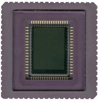
BOARD EVAL IMAGE SENS IBIS4-6600
Manufacturer
Cypress Semiconductor Corp
Datasheet
1.CYII4SC6600-EVAL.pdf
(34 pages)
Specifications of CYII4SM6600-EVAL
Sensor Type
CMOS Imaging, Monochrome
Sensing Range
6.6 Megapixel
Interface
SPI
Sensitivity
89 fps
Voltage - Supply
2.5 V ~ 3.3 V
Embedded
No
Utilized Ic / Part
IBIS4-6600
Lead Free Status / RoHS Status
Contains lead / RoHS non-compliant
Lead Free Status / RoHS Status
Lead free / RoHS Compliant, Contains lead / RoHS non-compliant


Assume that V
Externally, the output range of DAC_raw can be changed by connecting a resistor Rcal to RCAL_DAC_OUT and applying a voltage
V
Special case:
R
Rcal = 0, Vcal = GND ............................. then V
A similar relation holds for the output range of DAC_DARK (RCAL_DAC_DARK can be used to tune the output range of this DAC).
Analog to Digital Converter
The IBIS4-6600 has a two 10-bit flash analog digital converters. The ADCs are electrically separated from the image sensor. The
inputs of the ADC must be tied externally to the outputs of the output amplifiers. One ADC samples the even columns and the other
samples the odd columns. Alternatively, one ADC can also sample all the pixels.
Table 5. ADC Specifications
Setting the ADC Reference Voltages
Figure 12. ADC Resistor Ladder
Document Number: 001-02366 Rev. *G
Input Range
Quantization
Nominal Data Rate
DNL(Linear Conversion Mode)
INL (Linear Conversion Mode)
Input Capacitance
Conversion Law
VHIGH_ADC ~ 1.5V
VLOW_ADC ~ 0.42V
cal
cal
. The output voltage V
= then V
out
outfull
VDDA_ADC
= V
GND
outfull
Parameter
is the voltage that depends on the bit values that are applied to the DAC and ranges from:
V
outfull
(for example, for DAC_fine)
out
RADC = 577 Ohm
0 :
of DAC_raw follows the relation (R = 10 k).
(
bit
150 Ohm (ESD)
277 Ohm
150 Ohm (ESD)
values
V
out
00000000
High reference voltage
Low reference voltage
used by ADC
used by ADC
out
Set by External Resistors
(Refer the section
10 Bits
20 Msamples/s
Typ. < 0.4 LSB RMS
Typ. < 3.5 LSB
< 2 pF
Linear/Gamma corrected
Internal
= V
2
R
)
R
outfull
R
/2
R
cal
VDDA
cal
V
outfull
1 (
The internal resistance has a value of approximately 577 . Only
277 of this internal resistance is actually used as reference for
the internal ADC. This causes the actual ADC voltage range to
become half of the voltage difference between VHIGH_ADC and
VLOW_ADC. This results in the values listed
external resistors.
Table 6. ADC Resistor Values
RVHIGH_ADC
RInternal
RVLOWADC
Setting the ADC Reference
2
Specification
1
8
Resistor
)
2
(
R
bit
values
R
R
cal
IBIS4-6600 CYII4SM6600AB
11111111
V
cal
Value ()
Voltages)
)
560
577
220
Table 6
Page 11 of 34
for the
[+] Feedback
Related parts for CYII4SM6600-EVAL
Image
Part Number
Description
Manufacturer
Datasheet
Request
R

Part Number:
Description:
Manufacturer:
Cypress Semiconductor Corp
Datasheet:
Part Number:
Description:
Manufacturer:
Cypress Semiconductor Corp
Datasheet:
Part Number:
Description:
Manufacturer:
Cypress Semiconductor Corp
Datasheet:
Part Number:
Description:
Manufacturer:
Cypress Semiconductor Corp
Datasheet:
Part Number:
Description:
Manufacturer:
Cypress Semiconductor Corp
Datasheet: