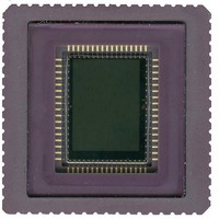
CYII4SM6600-EVAL Cypress Semiconductor Corp, CYII4SM6600-EVAL Datasheet - Page 21

CYII4SM6600-EVAL
Manufacturer Part Number
CYII4SM6600-EVAL
Description
BOARD EVAL IMAGE SENS IBIS4-6600
Manufacturer
Cypress Semiconductor Corp
Datasheet
1.CYII4SC6600-EVAL.pdf
(34 pages)
Specifications of CYII4SM6600-EVAL
Sensor Type
CMOS Imaging, Monochrome
Sensing Range
6.6 Megapixel
Interface
SPI
Sensitivity
89 fps
Voltage - Supply
2.5 V ~ 3.3 V
Embedded
No
Utilized Ic / Part
IBIS4-6600
Lead Free Status / RoHS Status
Contains lead / RoHS non-compliant
Lead Free Status / RoHS Status
Lead free / RoHS Compliant, Contains lead / RoHS non-compliant
Treg_int: Difference between left and right pointer = integration
counter until value "n" of INT_TIME register is reached =
INT_TIME register
In case of NDR = 0, the actual integration time Tint is given by
TintL: Integration time [# lines] = NROF_LINES register - INT_TIME
register + 1
In case of NDR = 1, NDR mode 1, the time Tint between two
readings of the same row is given by:
Tint:Integration time [# lines] = NROF_LINES register + 1
Table 13. Added Delay by Changing the DELAY Register Settings
X_REG Register
The X_REG register determines the start position of the window
in the X-direction. In this direction, there are 2208 + 2 + 12
readable pixels. In the active pixel array, sub sampling blocks are
24 pixels wide and the columns are read two by two. Therefore,
the number of start positions equals 2208/24 +2/2 +12/2 = 92 +
1 + 6 = 99.
Y_REG Register
The Y_REG register determines the start position of the window
in the Y-direction. In this direction, there are 3000 + 2 + 12
readable pixels. In the active pixel array, sub sampling blocks are
24 pixels wide and the rows are read one by one. Therefore, the
number of start positions equals 3000/24 + 2/2 +12 = 125 + 1 +
12 = 138.
Document Number: 001-02366 Rev. *G
0000
0001
0010
0100
0101
0011
0110
0111
Bits
Delay [# SYS_CLOCK periods]
shift-register
Sync of left
0
0
0
1
2
3
4
5
Line n
Figure 20. Syncing of Y-shift Registers
Sync of right
shift-register
1000
1001
1010
1011
1100
1101
1110
1111
Bits
In case of NDR = 1, NDR mode 2, the times Tint1 and Tint2
between two readings of the same row (alternatingly) are given
by:
Tint1: Integration time [# lines] = 2 * INT_TIME register + 1
Tint2: Integration time [# lines] = 2 * (NROF_LINES register + 1) - (2
* INT_TIME register + 1)
DELAY Register
The DELAY register can be used to delay the PIXEL_VALID
pulse (bits 0:3) and the EOL/EOF pulses (bits 4:7) to synchronize
them to the real pixel values at the analog output or the ADC
output (which give additional delays depending on their settings).
The bit settings and corresponding delay are indicated in
Table
Image_core Register
Bits 0:1 of the IMAGE_CORE register defines the several test
modes of the image core. Setting 00 is the default and normal
operation mode. If the bit is set to 1, the odd (bit 0) or even (bit
1) columns are tight to V
tune the sampling point of the ADCs to an optimal position.
Bits 2:7 of the IMAGE_CORE register define the sub sampling
mode in the X-direction (bits 2:4) and in the Y-direction (bits 5:7).
The sub sampling modes and corresponding bit setting are given
in the section
13.
Delay [# SYS_CLOCK periods]
T
reg_int
Sync
Analog to Digital Converter
Last line, followed by
sync of left shift-register
IBIS4-6600 CYII4SM6600AB
10
12
13
11
6
7
8
9
DD
. These test modes can be used to
on page 11.
T
int
Page 21 of 34
[+] Feedback


