CYII4SM6600-EVAL Cypress Semiconductor Corp, CYII4SM6600-EVAL Datasheet - Page 27
CYII4SM6600-EVAL
Manufacturer Part Number
CYII4SM6600-EVAL
Description
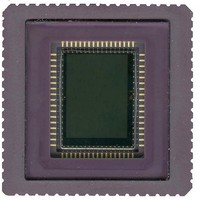
BOARD EVAL IMAGE SENS IBIS4-6600
Manufacturer
Cypress Semiconductor Corp
Datasheet
1.CYII4SC6600-EVAL.pdf
(34 pages)
Specifications of CYII4SM6600-EVAL
Sensor Type
CMOS Imaging, Monochrome
Sensing Range
6.6 Megapixel
Interface
SPI
Sensitivity
89 fps
Voltage - Supply
2.5 V ~ 3.3 V
Embedded
No
Utilized Ic / Part
IBIS4-6600
Lead Free Status / RoHS Status
Contains lead / RoHS non-compliant
Lead Free Status / RoHS Status
Lead free / RoHS Compliant, Contains lead / RoHS non-compliant


Pin Information
The following table lists all the pins and their functions. There are a total of 68 pins. All pins with the same name can be connected
together.
Table 15. Pin List
Document Number: 001-02366 Rev. *G
1
2
3
4
5
6
7
8
9
10
11
12
13
14
15
16
17
18
19
20
21
22
23
24
25
26
27
28
Pin
CMD_COL_CTU
CMD_COL
CMD_COLAMP
CMD_COLAMP_CTU
RCAL_DAC_DARK
RCAL_DAC_OUT
V
GNDA
V
GNDD
CMD_OUT_1
CMD_OUT_2
CMD_OUT_3
SPI_CLK
SPI_DATA
VDDAMP
CMD_FS_ADC
CMD_SS_ADC
CMD_AMP_ADC
GNDAMP
OUT1
ADC_IN1
VDDAMP
OUT2
ADC_IN2
V
GNDD
GNDA
DDA
DDD
DDD
Pin Name
Pin Type
Ground
Output
Output
Power
Power
Power
Power
Power
Power
Power
Power
Power
Input
Input
Input
Input
Input
Input
Input
Input
Input
Input
Input
Input
Input
Input
Input
input
0
1.08
0.66
0.37
1.27 at code 128
DAC_DARK reg
0
2.5
0
2.5
0
0.78
0.97
0.67
-
-
2.5
0.73
0.73
0.59
0
Black level: 1 at code 190
DAC_RAW register
See OUT1.
2.5
Black level: 1 at code 190
DAC_RAW register
See OUT2.
2.5
0
0
Expected Voltage [V]
Biasing of columns (ctu). Decouple with 100 nF to GNDA.
Biasing of columns. Connect to V
decouple to GNDA with C = 100 nF.
Biasing of column amplifiers. Connect to V
R = 100 k and decouple to GNDA with C = 100 nF.
Biasing of column amplifiers. Connect to V
R = 10 M and decouple to GNDA with C = 100 nF.
Biasing of DAC for dark reference. Can be used to set output
range of DAC.
Default: Decouple to GNDA with C = 100 nF
Biasing of DAC for output dark level. Can be used to set output
range of DAC. Default: Connect to GNDA
V
GND (&substrate) of analog part
V
GND (&substrate) of digital part
Biasing of first stage output amplifiers. Connect to VDDAMP
with R = 50 k and decouple to GNDAMP with C = 100 nF.
Biasing of second stage output amplifiers. Connect to
VDDAMP with R = 25 k and decouple to GNDAMP with
C = 100 nF.
Biasing of third stage output amplifiers. Connect to VDDAMP
with R = 100 k and decouple to GNDAMP with C = 100 nF.
Clock of digital parameter upload. Shifts on rising edge.
Serial address and data input. 16-bit word. Address first. MSB
first.
V
Biasing of first stage ADC. Connect to VDDA_ADC with
R = 50 k and decouple to GNDA_ADC with C = 100 nF.
Biasing of second stage ADC. Connect to VDDA_ADC with
R = 50 k and decouple to GNDA_ADC.
Biasing of input stage ADC. Connect to VDDA_ADC with
R = 180 k and decouple to GNDA_ADC with C = 100 nF.
GND (&substrate) of analog output
Analog output 1
Analog input ADC 1
V
Analog output 2
Analog input ADC 2
V
GND (&substrate) of digital part
GND (&substrate) of analog part
DD
DD
DD
DD
DD
of analog part [2.5V]
of digital part [2.5V]
of analog output [2.5V] (Can be connected to V
of analog output [2.5V] (Can be connected to V
of digital part [2.5V]
IBIS4-6600 CYII4SM6600AB
Pin Description
DDA
with R = 10 k and
DDA
DDA
Page 27 of 34
with
with
DDA
DDA
)
)
[+] Feedback
Related parts for CYII4SM6600-EVAL
Image
Part Number
Description
Manufacturer
Datasheet
Request
R

Part Number:
Description:
Manufacturer:
Cypress Semiconductor Corp
Datasheet:
Part Number:
Description:
Manufacturer:
Cypress Semiconductor Corp
Datasheet:
Part Number:
Description:
Manufacturer:
Cypress Semiconductor Corp
Datasheet:
Part Number:
Description:
Manufacturer:
Cypress Semiconductor Corp
Datasheet:
Part Number:
Description:
Manufacturer:
Cypress Semiconductor Corp
Datasheet: