C8051F360DK Silicon Laboratories Inc, C8051F360DK Datasheet - Page 178
C8051F360DK
Manufacturer Part Number
C8051F360DK
Description
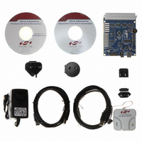
KIT DEV FOR C8051F360 FAMILY
Manufacturer
Silicon Laboratories Inc
Type
MCUr
Specifications of C8051F360DK
Contents
Evaluation Board, Power Supply, USB Cables, Adapter and Documentation
Processor To Be Evaluated
C8051F36x
Interface Type
USB
Lead Free Status / RoHS Status
Lead free / RoHS Compliant
For Use With/related Products
C8051F360, F361, F362, F363, F364, F365, F366, F367, F368, F369
Lead Free Status / Rohs Status
Lead free / RoHS Compliant
Other names
336-1410


C8051F360/1/2/3/4/5/6/7/8/9
16.8. Phase-Locked Loop (PLL)
A Phase-Locked-Loop (PLL) is included, which is used to multiply the internal oscillator or an external
clock source to achieve higher CPU operating frequencies. The PLL circuitry is designed to produce an
output frequency between 25 MHz and 100 MHz, from a divided reference frequency between 5 MHz and
30 MHz. A block diagram of the PLL is shown in Figure 16.3.
16.8.1. PLL Input Clock and Pre-divider
The PLL circuitry can derive its reference clock from either the internal oscillator or an external clock
source. The PLLSRC bit (PLL0CN.2) controls which clock source is used for the reference clock (see SFR
Definition 16.6). If PLLSRC is set to ‘0’, the internal oscillator source is used. Note that the internal oscilla-
tor divide factor (as specified by bits IFCN1-0 in register OSCICN) will also apply to this clock. When
PLLSRC is set to ‘1’, an external oscillator source will be used. The external oscillator should be active and
settled before it is selected as a reference clock for the PLL circuit. The reference clock is divided down
prior to the PLL circuit, according to the contents of the PLLM4-0 bits in the PLL Pre-divider Register
(PLL0DIV), shown in SFR Definition 16.7.
16.8.2. PLL Multiplication and Output Clock
The PLL circuitry will multiply the divided reference clock by the multiplication factor stored in the
PLL0MUL register shown in SFR Definition 16.8. To accomplish this, it uses a feedback loop consisting of
a phase/frequency detector, a loop filter, and a current-controlled oscillator (ICO). It is important to config-
ure the loop filter and the ICO for the correct frequency ranges. The PLLLP3–0 bits (PLL0FLT.3–0) should
be set according to the divided reference clock frequency. Likewise, the PLLICO1–0 bits (PLL0FLT.5–4)
should be set according to the desired output frequency range. SFR Definition 16.9 describes the proper
settings to use for the PLLLP3–0 and PLLICO1–0 bits. When the PLL is locked and stable at the desired
frequency, the PLLLCK bit (PLL0CN.5) will be set to a ‘1’. The resulting PLL frequency will be set accord-
ing to the equation:
Where “Reference Frequency” is the selected source clock frequency, PLLN is the PLL Multiplier, and
PLLM is the PLL Pre-divider.
178
Oscillator
Oscillator
External
Internal
PLL Frequency
Figure 16.3. PLL Block Diagram
0
1
PLL0DIV
÷
Reference
Divided
Clock
=
Reference Frequency
Rev. 1.0
Frequency
Detection
PLL0CN
Phase /
PLL0MUL
Loop Filter
÷
PLL0FLT
×
-------------- -
PLLM
PLLN
Controlled
Oscillator
Current
PLL Clock
Output
Related parts for C8051F360DK
Image
Part Number
Description
Manufacturer
Datasheet
Request
R

Part Number:
Description:
SMD/C°/SINGLE-ENDED OUTPUT SILICON OSCILLATOR
Manufacturer:
Silicon Laboratories Inc
Part Number:
Description:
Manufacturer:
Silicon Laboratories Inc
Datasheet:
Part Number:
Description:
N/A N/A/SI4010 AES KEYFOB DEMO WITH LCD RX
Manufacturer:
Silicon Laboratories Inc
Datasheet:
Part Number:
Description:
N/A N/A/SI4010 SIMPLIFIED KEY FOB DEMO WITH LED RX
Manufacturer:
Silicon Laboratories Inc
Datasheet:
Part Number:
Description:
N/A/-40 TO 85 OC/EZLINK MODULE; F930/4432 HIGH BAND (REV E/B1)
Manufacturer:
Silicon Laboratories Inc
Part Number:
Description:
EZLink Module; F930/4432 Low Band (rev e/B1)
Manufacturer:
Silicon Laboratories Inc
Part Number:
Description:
I°/4460 10 DBM RADIO TEST CARD 434 MHZ
Manufacturer:
Silicon Laboratories Inc
Part Number:
Description:
I°/4461 14 DBM RADIO TEST CARD 868 MHZ
Manufacturer:
Silicon Laboratories Inc
Part Number:
Description:
I°/4463 20 DBM RFSWITCH RADIO TEST CARD 460 MHZ
Manufacturer:
Silicon Laboratories Inc
Part Number:
Description:
I°/4463 20 DBM RADIO TEST CARD 868 MHZ
Manufacturer:
Silicon Laboratories Inc
Part Number:
Description:
I°/4463 27 DBM RADIO TEST CARD 868 MHZ
Manufacturer:
Silicon Laboratories Inc
Part Number:
Description:
I°/4463 SKYWORKS 30 DBM RADIO TEST CARD 915 MHZ
Manufacturer:
Silicon Laboratories Inc
Part Number:
Description:
N/A N/A/-40 TO 85 OC/4463 RFMD 30 DBM RADIO TEST CARD 915 MHZ
Manufacturer:
Silicon Laboratories Inc
Part Number:
Description:
I°/4463 20 DBM RADIO TEST CARD 169 MHZ
Manufacturer:
Silicon Laboratories Inc