C8051F360DK Silicon Laboratories Inc, C8051F360DK Datasheet - Page 51
C8051F360DK
Manufacturer Part Number
C8051F360DK
Description
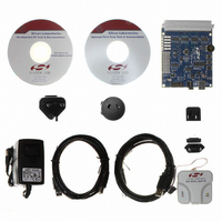
KIT DEV FOR C8051F360 FAMILY
Manufacturer
Silicon Laboratories Inc
Type
MCUr
Specifications of C8051F360DK
Contents
Evaluation Board, Power Supply, USB Cables, Adapter and Documentation
Processor To Be Evaluated
C8051F36x
Interface Type
USB
Lead Free Status / RoHS Status
Lead free / RoHS Compliant
For Use With/related Products
C8051F360, F361, F362, F363, F364, F365, F366, F367, F368, F369
Lead Free Status / Rohs Status
Lead free / RoHS Compliant
Other names
336-1410


5.3.
ADC0 has a maximum conversion speed of 200 ksps. The ADC0 conversion clock is a divided version of
the system clock, determined by the AD0SC bits in the ADC0CF register (system clock divided by
(AD0SC + 1) for 0 ≤ AD0SC ≤ 31).
5.3.1. Starting a Conversion
A conversion can be initiated in one of five ways, depending on the programmed states of the ADC0 Start
of Conversion Mode bits (AD0CM2-0) in register ADC0CN. Conversions may be initiated by one of the fol-
lowing:
Writing a ‘1’ to AD0BUSY provides software control of ADC0 whereby conversions are performed "on-
demand". During conversion, the AD0BUSY bit is set to logic ‘1’ and reset to logic ‘0’ when the conversion
is complete. The falling edge of AD0BUSY triggers an interrupt (when enabled) and sets the ADC0 inter-
rupt flag (AD0INT). Note: When polling for ADC conversion completions, the ADC0 interrupt flag (AD0INT)
should be used. Converted data is available in the ADC0 data registers, ADC0H:ADC0L, when bit AD0INT
is logic ‘1’. Note that when Timer 2 or Timer 3 overflows are used as the conversion source, Low Byte over-
flows are used if Timer 2/3 is in 8-bit mode; High byte overflows are used if Timer 2/3 is in 16-bit mode. See
Section “21. Timers” on page 247 for timer configuration.
Important Note About Using CNVSTR: The CNVSTR input pin also functions as Port pin P0.7 on the
C8051F360 devices and Port pin P0.6 on the C8051F361/2/6/7/8/9 devices. When the CNVSTR input is
used as the ADC0 conversion source, the corresponding port pin should be skipped by the Digital Cross-
bar. To configure the Crossbar to skip the port pin, set the appropriate bit to ‘1’ in register P0SKIP. See
Section “17. Port Input/Output” on page 183 for details on Port I/O configuration.
Modes of Operation
1. Writing a ‘1’ to the AD0BUSY bit of register ADC0CN
2. A Timer 0 overflow (i.e., timed continuous conversions)
3. A Timer 2 overflow
4. A Timer 1 overflow
5. A rising edge on the CNVSTR input signal
6. A Timer 3 overflow
C8051F360/1/2/3/4/5/6/7/8/9
Rev. 1.0
51
Related parts for C8051F360DK
Image
Part Number
Description
Manufacturer
Datasheet
Request
R

Part Number:
Description:
SMD/C°/SINGLE-ENDED OUTPUT SILICON OSCILLATOR
Manufacturer:
Silicon Laboratories Inc
Part Number:
Description:
Manufacturer:
Silicon Laboratories Inc
Datasheet:
Part Number:
Description:
N/A N/A/SI4010 AES KEYFOB DEMO WITH LCD RX
Manufacturer:
Silicon Laboratories Inc
Datasheet:
Part Number:
Description:
N/A N/A/SI4010 SIMPLIFIED KEY FOB DEMO WITH LED RX
Manufacturer:
Silicon Laboratories Inc
Datasheet:
Part Number:
Description:
N/A/-40 TO 85 OC/EZLINK MODULE; F930/4432 HIGH BAND (REV E/B1)
Manufacturer:
Silicon Laboratories Inc
Part Number:
Description:
EZLink Module; F930/4432 Low Band (rev e/B1)
Manufacturer:
Silicon Laboratories Inc
Part Number:
Description:
I°/4460 10 DBM RADIO TEST CARD 434 MHZ
Manufacturer:
Silicon Laboratories Inc
Part Number:
Description:
I°/4461 14 DBM RADIO TEST CARD 868 MHZ
Manufacturer:
Silicon Laboratories Inc
Part Number:
Description:
I°/4463 20 DBM RFSWITCH RADIO TEST CARD 460 MHZ
Manufacturer:
Silicon Laboratories Inc
Part Number:
Description:
I°/4463 20 DBM RADIO TEST CARD 868 MHZ
Manufacturer:
Silicon Laboratories Inc
Part Number:
Description:
I°/4463 27 DBM RADIO TEST CARD 868 MHZ
Manufacturer:
Silicon Laboratories Inc
Part Number:
Description:
I°/4463 SKYWORKS 30 DBM RADIO TEST CARD 915 MHZ
Manufacturer:
Silicon Laboratories Inc
Part Number:
Description:
N/A N/A/-40 TO 85 OC/4463 RFMD 30 DBM RADIO TEST CARD 915 MHZ
Manufacturer:
Silicon Laboratories Inc
Part Number:
Description:
I°/4463 20 DBM RADIO TEST CARD 169 MHZ
Manufacturer:
Silicon Laboratories Inc