ATAVRSB100 Atmel, ATAVRSB100 Datasheet - Page 13
ATAVRSB100
Manufacturer Part Number
ATAVRSB100
Description
SMART BATTERY DEVELOPMENT KIT
Manufacturer
Atmel
Type
Smart Batteryr
Datasheet
1.ATAVRSB100.pdf
(20 pages)
Specifications of ATAVRSB100
Contents
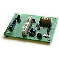
Fully Assembled Evaluation Board
Processor
ATmega406
Processor To Be Evaluated
ATmega406
Data Bus Width
8 bit
Interface Type
JTAG
For Use With/related Products
ATmega406
Lead Free Status / RoHS Status
Contains lead / RoHS non-compliant
Other names
Q2367281


2.7 General Settings and Functionality
2.7.1 Factory default settings
2.7.2 Switches and LEDs
2598C-AVR-06/06
device. This is jumpable directly on JB2 pins 3 and 4. Any other line that supports the
Pin-Change functionality could also be used.
As supplied from the factory, the ATAVRSB100 Development Kit is set up for
simulation of both cell voltages and pack current. The jumpers come configured as
shown in Table 2-7.
Table 2-7. Jumper settings on the SB100.
The SB100 board includes five LEDs that can be used for any purpose, but are
typically used as charge indicators. Additionally a pushbutton (SW1) is available for
activating this display function. JB1 provides the ability to isolate the I/O signals that
have been designated as LED control lines, if desired. When jumped, individual LEDs
are controlled by driving the associated I/O signal low. The JB1 pins are described in
Table 2-8 below.
The source voltage for the LEDs can come either from the 3.3V supply, or from PB6.
PB6 may be configured to act either as a standard I/O signal, enabling the LEDs
when driven high, or may optionally present the OC0A PWM output. Thus, OC0A may
be used to provide brightness control for the LEDs automatically in hardware. Note
that the PWM will power the LEDs during the high portion of the output signal.
It is highly recommended that the LEDs be lit one at a time, rather than enabled all
together, in order to reduce power supply current since the internal regulator of the
ATmega406 is limited. This solution is implemented in the OC0A Compare Match
Jumper
J1
JB1
JB2
JB3
JB4
HDR1
Description
Jumper present but not installed; used to provide BATT signal from cell side to
simulate the presence of a charger without requiring connectivity to a Host
system.
All five jumpers are installed to provide LED connectivity.
•
•
•
All five jumpers are installed (short pin 1 to pin 2, pin 3 to pin 4 and so on) to
enable cell voltage simulation.
Default connection to use simulator shunt for current measurement:
•
•
To use the R7 shunt resistor, typically when using actual battery:
•
•
Short pin 1 and 2 to connect PA0, which is ADC input, to all thermistors.
Short pin 3 and 4 to connect PA6 to SMBCLK, which is required for
Master-mode SMBus operation.
Short pin 5 and 6 to connect PA7 to Switch SW1, which is used for
activating LED function via button.
Short pin 7 and 8 to connect PB6 to LEDs (LED1:5), to adjust LED power
and intensity via OC0A PWM function.
Short pin 3 and 5 to connect SENSEHI line to Pack Current Simulation
(adjustable shunt resistance) VR6.
Short pin 4 and 6 to connect SENSELOW to GND (on connector
CONN2).
Short pin 1 and 3 to connect SENSEHI line to high side of R7
Short pin 2 and 4 to connect SENSELO line to low side of R7
AVR454
13
Related parts for ATAVRSB100
Image
Part Number
Description
Manufacturer
Datasheet
Request
R

Part Number:
Description:
DEV KIT FOR AVR/AVR32
Manufacturer:
Atmel
Datasheet:

Part Number:
Description:
INTERVAL AND WIPE/WASH WIPER CONTROL IC WITH DELAY
Manufacturer:
ATMEL Corporation
Datasheet:
Part Number:
Description:
Low-Voltage Voice-Switched IC for Hands-Free Operation
Manufacturer:
ATMEL Corporation
Datasheet:
Part Number:
Description:
MONOLITHIC INTEGRATED FEATUREPHONE CIRCUIT
Manufacturer:
ATMEL Corporation
Datasheet:
Part Number:
Description:
AM-FM Receiver IC U4255BM-M
Manufacturer:
ATMEL Corporation
Datasheet:
Part Number:
Description:
Monolithic Integrated Feature Phone Circuit
Manufacturer:
ATMEL Corporation
Datasheet:
Part Number:
Description:
Multistandard Video-IF and Quasi Parallel Sound Processing
Manufacturer:
ATMEL Corporation
Datasheet:
Part Number:
Description:
High-performance EE PLD
Manufacturer:
ATMEL Corporation
Datasheet:
Part Number:
Description:
8-bit Flash Microcontroller
Manufacturer:
ATMEL Corporation
Datasheet:
Part Number:
Description:
2-Wire Serial EEPROM
Manufacturer:
ATMEL Corporation
Datasheet: