ATAVRSB100 Atmel, ATAVRSB100 Datasheet - Page 8
ATAVRSB100
Manufacturer Part Number
ATAVRSB100
Description
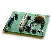
SMART BATTERY DEVELOPMENT KIT
Manufacturer
Atmel
Type
Smart Batteryr
Datasheet
1.ATAVRSB100.pdf
(20 pages)
Specifications of ATAVRSB100
Contents
Fully Assembled Evaluation Board
Processor
ATmega406
Processor To Be Evaluated
ATmega406
Data Bus Width
8 bit
Interface Type
JTAG
For Use With/related Products
ATmega406
Lead Free Status / RoHS Status
Contains lead / RoHS non-compliant
Other names
Q2367281


2.2 Using the simulator stages
2.2.1 Calibrating the Cell Simulator
8
AVR454
Table 2-6. Test points on SB100
This chapter describes how to calibrate and use the integrated voltage simulator, and
also how to use the current simulator.
Calibration of the Cell Simulator section is actually very easy due to the design of the
circuitry. Since each cell’s potentiometer can be independently adjusted without
affecting the others, calibration does not require a great deal of back-and-forth
adjustment to take place.
Due to component tolerances, the upper range of adjustment will typically exceed
what can be tolerated by the ATmega406, namely, 5.5V. Care should therefore be
taken not to exceed the ATmega406 voltage ratings during calibration and during
development.
For most users it will be helpful to have all four cell simulation potentiometers
adjusted to the same setting, with the ability to adjust each cell slightly upward if
desired before reaching the upper end of the adjustment. This procedure will
establish that setting.
1. Wire up the CONN2 terminal strip for simulation as indicated in Figure 2-3.
2. Install all five jumpers on JB3.
3. Adjust V-SIM1-4 (VR1-4) fully counter-clockwise to their minimum setting. The
4. Apply 24.0VDC to the designated V-SIM supply terminals (not to the I-SIM
5. Adjust V-SIM Range Adjust (VR5) fully clockwise. This supplies the maximum
6. Measure across CELL1+/CELL1- terminals while adjusting V-SIM1 clockwise to
7. Repeat step 6 for cells 2-4.
After calibration, the main power supply voltage can be reduced if so desired, as low
as the maximum cell stack voltage plus 2.0VDC. Before making this adjustment, VR5
should be reduced to match the maximum stack voltage. For example, if the
maximum cell voltage desired is 4.2VDC, and a four-cell stack is used, adjust VR5 to
produce
can then be reduced from 24V to 18.8V.
Test Point Name
TP1
TP2
TP3
potentiometers are 12-turn, and one can hear a low click when end settings are
reached and every full turn from thereafter.
terminals!). Do not exceed 24.5VDC to the board at any time! Ensure that you have
a ripple-free DC supply available. Some wall converters that are DC-rated do not
include a filter capacitor and only output pulsed DC, which is not acceptable for
use.
current into the simulation pots.
reach 5.25VDC.
4
2 .
V
⋅
4
=
16
Description
Test Point 1 is the junction between the two primary power MOSFET
devices, Q3 and Q4, and is provided for testability purposes only.
Test Point 2 is the Vref output signal. If enabled and calibrated, this
should have 1.100VDC present.
Test Point 3 is the BATT signal, after passing through a dual diode
device to allow enabling this signal from either a cell-side or a host-
side power source. It is provided for testability purposes only.
8 .
V
across the stack (CELL4+ to CELL1-). The power supply
2598C-AVR-06/06
Related parts for ATAVRSB100
Image
Part Number
Description
Manufacturer
Datasheet
Request
R

Part Number:
Description:
DEV KIT FOR AVR/AVR32
Manufacturer:
Atmel
Datasheet:

Part Number:
Description:
INTERVAL AND WIPE/WASH WIPER CONTROL IC WITH DELAY
Manufacturer:
ATMEL Corporation
Datasheet:
Part Number:
Description:
Low-Voltage Voice-Switched IC for Hands-Free Operation
Manufacturer:
ATMEL Corporation
Datasheet:
Part Number:
Description:
MONOLITHIC INTEGRATED FEATUREPHONE CIRCUIT
Manufacturer:
ATMEL Corporation
Datasheet:
Part Number:
Description:
AM-FM Receiver IC U4255BM-M
Manufacturer:
ATMEL Corporation
Datasheet:
Part Number:
Description:
Monolithic Integrated Feature Phone Circuit
Manufacturer:
ATMEL Corporation
Datasheet:
Part Number:
Description:
Multistandard Video-IF and Quasi Parallel Sound Processing
Manufacturer:
ATMEL Corporation
Datasheet:
Part Number:
Description:
High-performance EE PLD
Manufacturer:
ATMEL Corporation
Datasheet:
Part Number:
Description:
8-bit Flash Microcontroller
Manufacturer:
ATMEL Corporation
Datasheet:
Part Number:
Description:
2-Wire Serial EEPROM
Manufacturer:
ATMEL Corporation
Datasheet: